|
The Pentode Amplifier
During the first parts of this series we have managed to introduce all of the most popular valve configurations and have provided an insight into their physical construction and development. We hope that some of the electrical theory, esoteric as it may at first appear, has not dissuaded anyone from experimenting with these devices. In practice it is usual for established circuit configurations to be applied to most types of valve, and reference to valve data literature usually reveals such circuits, thus making valve circuit building much easier. In the meantime we shall continue with the experimentation and discuss a practical pentode amplifier. The term 'pentode amplifier' will be used here to embrace circuits which also employ beam tetrodes as well, since the design principles are essentially the same for both types of valve. However, when comparing the design approach of the above with that for triodes, some significant differences will be found, in addition to the obviously greater circuit complexity of the pentode arrangement. Previously it was pointed out that one significant difference between the triode and the pentode is the fact that the latter has a very much higher value of ra than the triode. It is this fact that changes the design approach.
The Pentode Amplifier Equivalent Circuit
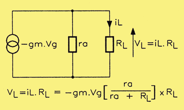
Constant current equivalent circuit for a pentode valve.
Because of the very high value of ra for pentodes, the equivalent circuit that is used is based on a constant current generator feeding into parallel resistors, the output from the circuit then being obtained from the product of a current and the effective load resistance. Thus, we start with so much available current which then divides between the parallel resistors, part of this current then being used to develop the output voltage. The idea is seen above, which shows the simplest possible constant current equivalent circuit for a pentode.
This equivalent circuit consists of three elements. The first of these, with the 'figure of eight' symbol, is the constant current generator itself. This represents the amplifying action of the valve and is seen to consist of the mutual conductance gm of the valve multiplied by the signal input voltage Vg; to this has been attached a minus sign. Dealing with the latter first, this is merely a way of stating that the valve inverts the input signal. With the load in the anode circuit there is always a phase shift of 180° between the input signal and the output signal. This is exactly the same situation as in transistor amplifiers of both the bipolar and field effect types – so there is nothing new here!
We know that gm = delta Ia / delta vg (where delta means a small change of), so if we are multiplying this by Vg itself, we shall get a current as the answer. To put some figures to this, if the input signal had a peak value of 0.5 V and the gm of the valve was 1.85 ma/V, then the magnitude of the constant current generator in the circuit, namely – gm.Vg, will equal 1.85 (mA/V) x 0.5 (V), which equals 0.925 mA (peak) of anode current.
The two parallel resistors in the circuit above, into which this total current of feeds, are the ra of the valve and the anode load resistor Rl itself. If we assume a value of ra of 2.5 MΩ, then it is merely left to assign a value to the anode load resistor in order to be able to calculate the gain stage and, hence, the value of the output voltage.
Determination of Anode Load
As for the triode, the voltage gain of stage is directly proportional to the value of the anode load. However, there is always an upper limit to the value of anode load resistor that can be used, since the flow of direct anode current through this load causes a DC voltage drop. The maximum permitted voltage drop value depends upon the value of the DC supply available, and the required standing value of the anode voltage. For example, if the DC supply is +250 V and the standing 'no signal' value is not to be less than 80 V, then the DC voltage drop across the anode load resistor under no signal conditions cannot exceed 250 V-80 V, namely 170 V. With a standing anode current of just 1 mA, the value of the anode load obviously is limited to 170 kΩ or less. Taking the first standard resistor value below this figure leads to a choice of 150 kΩ for the anode load. This is quite small compared with the value of ra quoted above, leading to the conclusion that most of the anode current in the circuit above will flow in the anode load resistor Rl.
A Useful Simplification
We could obviously work out just how much of our constant current of 0.925 mA would flow in the 150 kΩ load resistor. We could employ the current divider principle for this, but it is not really necessary since here is a simple approximation that can be used. This is derived as follows, and is based on the assumption that the ra of the valve is much greater than the value of the anode load resistor. The circuit diagram includes the formula for calculating the output voltage Vl across Rl using the current divider principle mentioned above and the fact that Vl = Il x Rl, This is repeated here as follows:–
Output voltage across
Rl = gmVg x ((ra) / (ra + Rl)) x Rl
If ra is much larger than Rl, then the bracketed term (ra + Rl) simplifies to just ra This allows ra in both numerator and denominator to be cancelled, leaving us with the following expression for the output voltage:–
Output voltage across
Rl = -gmVg x Rl (Equation one a)
This in turn leads to a simple expression for voltage gain for pentode amplifiers; if we divide both sides by the input signal voltage, Vg:–
Voltage gain (VAF) = -gm x Rl (Equation two)
We can now apply the above formulae to the specific case above, where we assigned values to the various parameters and circuit constants.
These were:–
gm = 1.85 mA/V; Vg = 0.5 V peak; Rl = 150 kΩ
Thus:–
Output voltage = -1.85 x 0.5 x 150, = -138.75 V. (using (Equation one a) above)
Voltage gain = -1.85 x 150 = -277.5 (using (Equation 2) above)
The above calculations should make it clear that the voltage gain of a pentode amplifier can be much greater than that of a triode amplifier, because of its ability to employ very much higher values of anode load. One may also state that the superior amplifying ability of the pentode arises because of its very much higher value amplification factor μ However, this is merely restating the above because μ = ra x gm and it is the higher value of ra that permits the higher value of Rl to be used.
Design of a Pentode Voltage Amplifier
The design of such an amplifier will have to take into account the supply voltage available. In the case of the power supply design offered in A Valve Power Supply within this series, this is limited to about 150 V. To be fair, this may seem a high voltage compared with the values that we associate with today's solid state circuits but, in terms of normal valve practice, it is actually quite low. Supply voltages of the order of 250 to 500 V are more usual. Nonetheless, valves will work quite happily down to much lower voltages and the value of 150 V, arrived at for our power supply design, was a result of considering the desirability of producing a stabilised supply of the simplest type. This led to the use of Zener diodes, the choice of these being dictated in turn by the types available, their power ratings, etc. A bit of a Catch 22 situation really.
If a higher, though un-stabilised supply is required, it can be obtained from the reservoir capacitor, where the DC level will be of the order of 340 V DC. In this event, most amplifier stages would have a series resistor and decoupling capacitor inserted into their supply rails to remove the supply ripple from the valve stage's actual HT supply, in effect an RC filter. Examination of commercial valve designs will show this approach to be very common. The design that follows should establish the basic principles, and other designs using different supply voltages should not be beyond the capabilities of the average experimenter.
The valve we are going to use for this experiment is the EF86, which, as with the ECC81 et al, comes with a B9A base and a thin glass tube envelope. The EF86 is a low noise, AF voltage amplifying pentode specifically for very small signal preamplifier applications. It features an all enclosing, outer screen or shield around all electrodes (connected to pins 2 and 7), special measures for extra mechanical stability against microphony, and a bifilar wound heater element to reduce hum injection to the absolute minimum.
The full Mullard data-sheet for the EF86 is available within the exhibit. A brief synopsis of the operating characteristics is presented below.
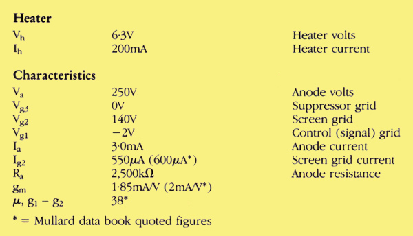
μ should we wish to know it, can be derived from the product of the other parameters. Before we leave the table, it ought to be mentioned that, as ever, the heater supply is 50 Hz AC sinusoidal (from the mains transformer) and so of course the values quoted are RMS. A valve base connection diagram is below.
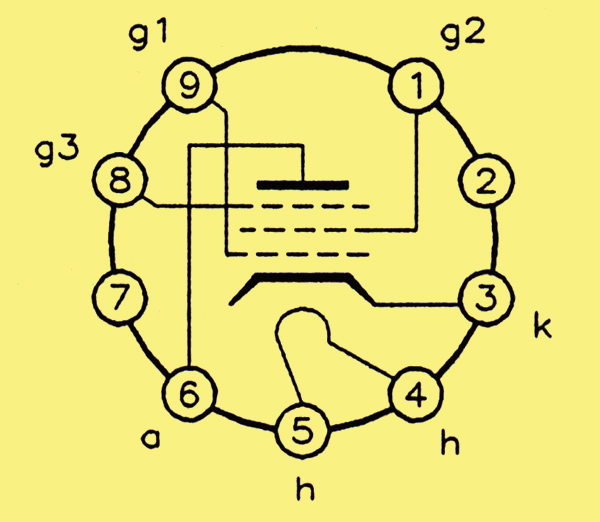
Pin-out diagram for the EF86 low-noise AF pentode valve (base viewed from below)
Back to μ though. Since μ = ra x gm; μ = 2,500 x 1.85; thus μ = 4,625. The parameter ra is in kΩ and gm is in mA/V, so these two can be multiplied directly to give the correct result.
As a starting point, we shall simply scale down the anode and screen data in proportion to the value of supply voltage available. Since the supply voltage is only 150 V to start off with, the anode voltage must be a good deal less than this.
Mentally, we say it could be about 100 V; this leads to the thought that, if we do use this value, there will then be a drop of 50 V across the anode load resistor. Another mental calculation follows based on the simple Ohm's law fact that:–
Voltage drop across anode load Rl = Ia x Rl.
This leads to the rather obvious deduction that Ia and Rl are mutually dependent and choosing one – for whatever criteria – automatically determines the other. Which should we choose first? Voltage gain depends upon the value of Rl, so let us assume that we need to have a voltage gain somewhere in the range 80 to 100 times and work out the required value of Rl that would give such a gain. From this we can determine the corresponding value of anode current Ia and decide whether the value calculated is a practical one.
Since VAF = gm x Rl,
then Rl = VAF/gm,
= 100/1.85 (using the upper limit of VAF),
= 54 kΩ (or 56 kΩ using nearest preferred value).
As already stated, the voltage drop across this load resistor is going to be about 50 V. The anode current value that would produce such a voltage drop can be calculated using Ohm's law, as follows:–
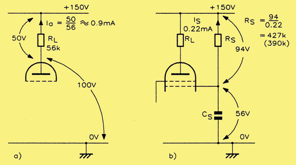
(a); calculating the value of R1 and the anode current Ia, (b); similar calculations for the screen dropper resistor.
Anode current = voltage drop across Rl/(value of Rl) = 50 V/56 kΩ, = 0.9 mA (approx).
This is a perfectly reasonable value for Ia, so the design can proceed on this basis. We now need to calculate the component values for setting the screen voltage and current. What should these be?
Again, we shall simply scale down the values given in the table in the same proportions as we scaled down the anode voltage, that is 2.5:1. On this basis, if Vs = 140 V and Is = 0.55 mA, then these become Vs = 56 V and Is = 0.22 mA, obtained by dividing the original values of Vs and Is by a factor of 2.5.
The screen voltage will be determined in the time honoured way by a resistor connecting the screen to supply HT+, with a decoupling capacitor from the screen down to 0 V. The value of the screen dropper resistor is determined simply by using Ohm's law. Since the screen voltage (with respect to 0 V) is 56 V, then the voltage drop across this resistor is equal to 150 - 56 V, which equals 94 V (see (b) above). With a screen current of 0.22 mA, the value of the screen dropper resistor will be equal to 94 V/0.22 mA, which equals 427 kΩ
The choice from the nearest preferred resistor values lies between 390 kΩ and 470 kΩ let us use the former as a starting point. We now have to determine the value for the decoupling capacitor from screen to 0 V. This value will be determined by the signal performance required of the amplifier. The topic is covered in depth in the old time classic Electronic and Radio Engineering by F E Terman (McGraw-Hill), in which the author discusses the loss of gain that results, due to negative feedback, if the bypassing action of the screen to ground capacitance is not complete. It is not necessary to get into this discussion in depth; we can just pick the bones out of it and arrive at a rule of thumb approach for a practical solution.
On the basis that (according to Terman) screen bypassing will be complete if the impedance of the screen bypass capacitor is substantially less than the value of the total effective screen impedance, at the lowest frequency of interest, then we can derive the following simple rule.
At the lowest working frequency, the screen bypass capacitor should have a reactance whose value is not greater than one-tenth of the value of the screen dropper resistor.
The full derivation is too complex to include here and requires a knowledge of the dynamic resistance, rs of the screen, which is not available. Its value is, however, usually a good deal less than the value of the screen dropper resistance. On this basis, it seemed safe to use the factor of 'one-tenth' given above.
If we assume that the lowest frequency of interest is, say, 20 Hz – a not unreasonable assumption for an audio-frequency amplifier – then we have to calculate a value of capacitance whose reactance is not greater than 390 kΩ/10 at this frequency.
Since Xc = l/(2.π.f.C),
then C = l/(2.π.f.Xc), = l/(2.π.20.39.10-3), = 1/4.9 μF, = 0.2 μF (or 0.22μF, using nearest preferred value)
Note that we have ended up with a perfectly reasonable value for the screen bypass capacitor.
In the case of the EF86, the suppressor grid is not internally connected and, therefore, in this design we shall strap it externally to the cathode. Nine times out of ten it would be connected like this anyway. We now come to the matter of the grid bias and here we are going to have to make an educated guess at the value of negative grid voltage required. All that we know is that, when the anode voltage is 250 V, -2 V on the grid gives an anode current of 3 mA, Since the anode characteristics for a pentode are nearly horizontal over a wide range of anode voltage, then .reducing the anode voltage from +250 V to +100 V should actually have very little effect on the anode current. However, we are also reducing the anode current requirement from 3 mA to 0.9 mA, an approximate 3:1 reduction and also reducing the screen voltage from +140 V to +56 V and this will have a significant effect on anode current. For a given grid bias voltage, reducing the screen voltage brings about a proportionate reduction in anode current. On this basis, we can probably safely leave the grid bias voltage at the value of -2 V already given and assume that the lower screen voltage used will automatically give us the lower value of the anode current that we need. If it does not quite achieve this, we need only modify the test circuit accordingly. Let us see how this works out. The value of the cathode bias resistor obtained by using Ohm's law, as follows. Cathode bias resistor = Grid bias voltage/total cathode current.
In the case of the triode the anode current and the cathode current are one and the same thing; in the case of the pentode they are not. For the pentode: Total cathode current = anode current + screen current.
In this specific case, total cathode current = 0.9 + 0.22 (mA), = 1.12 mA.
Since the required grid bias voltage, Vg, = 2 V, then the value of the cathode bias resistor is equal to 2 V/1.12 mA, which equals 1.8 kΩ (very nearly). This will need to be bypassed by a capacitor whose value is chosen in a similar manner to that of the screen bypass capacitor, namely that its reactance at the lowest signal frequency (20 Hz in this case) is not greater than one-tenth of the cathode bias resistor value. This can be expressed by the formula:–
C = l/(2π.20.l08) = 44.2 μF (or 47 μF, using nearest preferred value).
The design is now essentially complete, the value for the grid leak resistor being the nominal 1 MΩ that is usually chosen. The input coupling capacitor will, of course, influence the bandwidth by determining the low frequency cut-off point. If this capacitor has a reactance equal to the resistance of the grid leak at 20 Hz, then 20 Hz becomes the lower -3 dB frequency.
Thus, we have one final calculation for capacitance:–
C = l/(2.π.20.l0-6) = 1/40π μF = 0.008 μF (or 0.01 μF (10 nF) using nearest preferred value). Thanks to Stig Comstedt for pointing out the errors in these articles. These range from the errors I introduced during OCR to the errors in the original article such as the input capacitance calculation that actually comes out to 10 nF and not the 100 F as in the diagram below.
The complete circuit for the pentode amplifier is shown below.
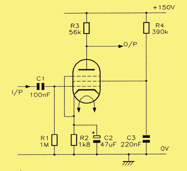
Circuit for the EF86 pentode amplifier designed in the text.
Hooking up the Amplifier
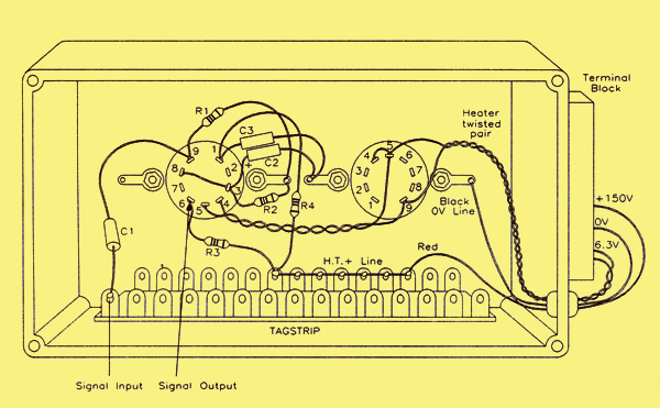
Under chassis layout for the pentode amplifier.
The same experimental chassis was used as previously and the under-chassis layout is shown above. Only one valve base is required, of course. Because the valve base nearer to the terminal block end of the chassis had its heaters wired for the double-triodes, I left this alone for future use and used the other base for the pentode, the heater supply for this valve being wired to pins 4 and 5. A further twisted pair extended the heater wiring from the heater connections of the first valve.
Testing the Amplifier
The first tests consisted of measuring the DC potentials at the relevant electrodes, to see how they compared with the design values. I expected some discrepancy here because of a lack of exact knowledge of the grid bias voltage required. The results were as follows:–
Anode voltage Va = +108 V; Screen voltage Vs = +94 V; Cathode voltage Vk = +2.1 V.
From this it seemed that, even though the valve was probably taking about the right total space current, the screen current was too low, which accounted for the higher than required value of static screen voltage. However, it was not considered vital to make significant changes to the screen components in order to get the screen voltage closer to its design value; for the record, increasing the screen dropper resistor to 470 kΩ caused a reduction in Vs and an increase in Va, with no effect on the dynamic performance of the amplifier.
With the DC values more or less acceptable, a signal input at 1 k Hz was connected to C1, the input coupling capacitor and the CRO used to monitor the input and output signal levels. It was found that the positive peak of the output signal began to round off noticeably at an output level of 62 V Pk-to-Pk. This is due to non-linearity of valve characteristics and underlines the fact that the theoretical output swings, described in some text books, approaching supply voltage values are just that – theoretical! As it happens, this imposes no limitation at all on the use of this valve since its application area is as a preamplifier of relatively low level signals (where the Pk-to-Pk values are only a few volts) and not as an output stage.
Comparison of the amplitudes of input and output signals revealed something of a disappointment. With an output of 50 V Pk-to-Pk, the input signal level was 0.8 V Pk-to-Pk, giving a voltage gain of just about 63 (36 dB), rather than the figure of 100 (40dB) hoped for. One can account for this by remembering that the values of gm and ra used in the calculations of gain made previously are subject to production 'spreads and, furthermore, were quoted in the data book at much higher levels of voltage and current (anode and screen). Working right down at the low end of the valve characteristics one can expect the slopes to be that much less and, consequently, the values of the parameters to be that much lower than further up (but 'Another Approach' below).
Measurement of Bandwidth
An electronic voltmeter with a decibel scale was used to monitor the output, which was adjusted so as to indicate at the 0 dB mark, on a convenient range, at the mid-band frequency of l kHz. Naturally, the CRO was used to check that the signal level was well below that which would produce distortion. The frequency was then progressively reduced until the voltmeter reading fell by 3 dB; the frequency was noted as 11 Hz, this being an improvement on the design value of 20 Hz. The frequency was then similarly increased until again the output fell by 3 dB; the frequency at which this occurred was noted at 16 kHz, not exactly a startlingly high frequency performance. With more development, this could be improved, a figure of 20 to 30 kHz being a more likely objective.
Summing Up
It is hoped that the procedure above has established a basic design approach to a single-stage pentode amplifier. The results I think, justify statements made earlier concerning the superiority of the pentode as a voltage amplifier, certainly in terms of higher gain at least. The results would undoubtedly be even more with a power supply capable of the higher voltages normally with such amplifiers in practice.
Another Approach
Using Mullard's Data and now, after all this, reference to Mullard application data for the EF86 (which Mullard designed) supplied an archetypal circuit configuration for an EF86 pentode amplifier, for which, they say, only two sets of resistor values need be decided, and from which, advise Mullard, you should not deviate. Using the amplifier circuit diagram again as a reference – this is, after all, the only circuit configuration that is practical for the EF86.
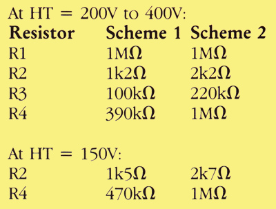
No tedious calculations of any sort are required on the part of the designer, he just builds the circuit. Either scheme works well for all HT levels from 150 V to 400 V. Scheme 1 is the commonest, and the stage is capable of signal gain exceeding 4O dB (>100 times, depending on HT level – the higher the better), with noise down to 2 μV. Try it and compare it with the calculated model. As is usual in these cases, the manufacturer is right and his recommendations are practically. impossible to improve on. It is for this reason that commercial valve circuits tend to resemble clones of each other; it is extremely difficult to be truly original when designing 'new' valve circuits, the valves themselves will not allow radical deviations. Scheme 2 is an extra-low noise, high gain configuration which might be used for very small signals, like tape playback head output. The actual value of R1 can be altered to match the impedance of the transducer -47 kΩ for a magnetic pick-up cartridge, for example.
However, on choosing these values, you must not then expect to be able to precisely set the biased DC anode voltage wherever you like. In practice the anode voltage will be roughly two thirds that of the HT supply with the values shown in the table. From the point of view that the primary function of the circuit is that of an AC amplifier, its exact DC conditions are of secondary importance.
|