|
This simple audio amplifier employs a beam tetrode output valve and a transistor voltage amplifier, thereby combining the advantages of Class A output and transistor hum-tree circuitry.
This was in 1971 before high performance op-amps. Looking on the internet in 2012 most commercial hybrid amps use a valve voltage amplifier and mosfet output stages. The pleasing 'valve' sound comes from the output stage not the gain stages - ed.
Although the writer looks upon the transistor as being a great improvement on the valve for most applications, he still hankers after the comfortably ample and trouble-free speaker drive which can be obtained from a simple Class A output beam tetrode. Transistor AF output stages seem to introduce complication upon complication, and even then the output is only in Class B! Unless they are employed in quite complex circuits, transistors do not seem to offer the clean low-distortion output that is given by the valve.
It was these thoughts which spurred the writer to develop the amplifier circuit which forms the subject of this short article. The amplifier is intended to operate from a mono crystal pick-up, from a radio tuner unit, or from any similar source offering an audio input at around the same voltage level. The output stage employs a 6BW6, which is the B9A equivalent of our old friend, the 6V6. Indeed, a 6V6 could be employed instead of the 6BW6, if desired. The 6BW6 is preceded by a transistor stage designed around a BC169C, this being a very high gain silicon transistor.
So far as the writer can see, the only disadvantage with the present amplifier, when compared with an all-transistor design, is that an HT voltage is required for the valve, whereupon high voltage electrolytic capacitors and a mains transformer with a high voltage HT secondary are needed. But a mains transformer would also be required for a transistor amplifier offering the same power output, and the smoothing capacitors for a transistor version, although having working voltages that are lower than those employed for a valve, would nevertheless have much higher capacitance values. Further, a voltage regulating circuit might be required as well. Thus, the use of a high voltage HT supply might not be such a big disadvantage after all.
Circuit
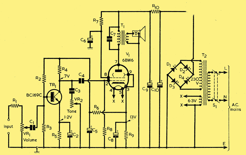
The circuit of the complete amplifier. The voltage figures at the transistor emitter and collector, and at the valve cathode, are discussed in the text
The circuit of the hybrid amplifier is given in the accompanying diagram. Here, the input signal is applied to R1 and VR1 in series, R1 being included to ensure that the input resistance is sufficiently high for crystal pick-ups. VR1 is the volume control and the signal tapped off by its slider is passed via C1 to the base of TR1. Since this transistor is required to function here as a voltage amplifier, it has a relatively high value of collector load, average collector current being approximately 0.5 mA. The transistor functions well at this low current, which is not excessively removed from the figure of 2 mA at which its hfe is specified. The amplified signal at the collector of TR1 is next fed, via C4, to the signal grid of the output valve, V1. C3 and VR2 form a variable top-cut tone control.
Cathode bias for V1 is developed across R9 in the usual manner. The cathode bias voltage is then employed as a DC supply for the transistor collector load and base bias network. It was considered advisable to decouple the transistor circuit from the cathode by means of R6 and C5.
The beam tetrode stage functions in conventional manner. In the writers version the screen-grid is fed via R7 and C6 but it is probable that there would be negligible change in performance if the screen-grid were taken directly to the upper end of T1 primary, thereby saving a resistor and an electrolytic capacitor. This alternative arrangement can be tried by constructors, if desired. Experiment is possible, also with capacitor C7, which may be changed in value or omitted altogether to suit individual tastes and speakers.
The speaker is 3Ω impedance, and the output transformer should have a ratio which allows an impedance of approximately 5,000Ω to be presented to the 6BW6 anode. The speaker transformer should also be rated at 4 Watts or more.
The HT rectifier and smoothing circuit is quite conventional, the mains transformer, T2, being an Osmabet component offering 230 Volts at 45 mA and 6.3 Volts at 1.5 amp. Rectifiers D1 to D4 can be silicon diodes type BY100, or they can consist of a single bridge rectifier rated at 250 Volts 45 mA or more, Suitable silicon bridge rectifiers are readily available rather than the metal rectifier specified in 1971.
The only remaining component is on-off switch S1. This is ganged with volume control VR1.
Assembly
The assembly of the amplifier raises few problems. Any suitable metal chassis may be employed, the most bulky items being T1 and T2. These should be mounted with their axes at right angles to each other. The choice of input and speaker terminals is left to the constructor. Probably the most convenient form for the input terminals is provided by a phono socket. The transistor circuitry should be kept away from mains and power supply wiring and components. It is, however, essential for the mains input wiring to pass to the on-off switch ganged with VR1, and this wiring should be routed such that it does not approach the transistor components too closely. These components can be assembled on tag-strips or tag-boards as desired. The transistor specified is a tiny device and it may be necessary to extend one or more of its leads by soldering on an extra length of wire, with thin sleeving passed over the joint. Take care not to heat the transistor excessively during soldering.
Operation
When the amplifier has been completed it may be tried out, whereupon it should provide a pleasant quality of reproduction at an ample volume level.
Before the amplifier can be considered finally complete it is necessary to take several voltage checks to ensure that the transistor is working on the correct part of its characteristic. The component values specified for R2 to R5 are such that the collector voltage should, working from experience with the writers amplifier, lie approximately mid-way between the voltage on the cathode of V1 and a potential 1 Volt positive of chassis. This allows the collector to swing symmetrically, with the audio signal, nearly to its supply potential (which is the cathode potential minus the very small voltage dropped in R6) in one direction, and nearly to its emitter potential (which is of the order of 1 Volt positive of chassis) in the other direction. A typical example of what is to be expected is given by the voltage figures given in the diagram, which show the potentials measured in the writers amplifier. Here, the valve cathode is 13 Volts positive of chassis, and the transistor collector is 7 Volts above chassis, as is required. It so happens that the potential on the emitter in this case is 1.2 Volts. If the cathode voltage had been 14 the collector voltage would need, ideally, to be 7.5, and if the cathode voltage had been 12 the collector voltage would need, ideally, to be 6.5, and so on. The collector voltage should be read by a valve voltmeter or by a test-meter with an internal resistance of at least 200,000Ω. The latter would be given by a 20,000Ω per volt instrument switched to read 10 Volts FSD, or by a 10,000Ω per volt instrument switched to read 20 Volts FSD. 21st century instruments normally have an input impedance of 10 MΩ and present a much lighter load on the circuit that the 20,000 Ω per volt of the AVO Model 8 et al.=
The cathode and collector voltage readings are taken under quiescent conditions. If it is found that the desired collector voltage, plus or minus some 0.5 Volt, is given with the components that have been fitted, then all is well and no further work is needed. If, on the other hand, the required voltage is not given, the discrepancy will be due to variations, within tolerance, of the resistors and the transistor. The value of R5 then has to be changed slightly until the appropriate collector voltage is given. Increasing the value of R5 causes the collector voltage to increase, and vice versa.
If a valve voltmeter or suitable test-meter is not available, the optimum value required in R5 can be determined in the following manner. Take a 5kΩ or 10kΩ linear track potentiometer, connect it temporarily into circuit in place of R5, and adjust it to offer a resistance slightly in excess of 2kΩ. Apply a high level signal to the amplifier and adjust the potentiometer in both directions to the settings which cause the same level of obvious distortion to be given. Then set the potentiometer carefully to the point which lies mid-way between these settings. Remove it from circuit, measure its resistance, then connect a fixed resistor of the same value in the R5 position.
Component List
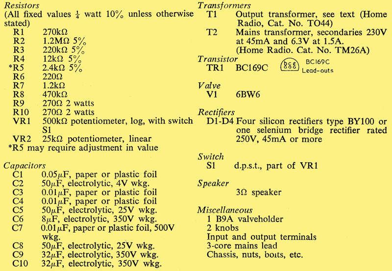
The original suppliers have been left in place although the companies may no longer exist.
|