|
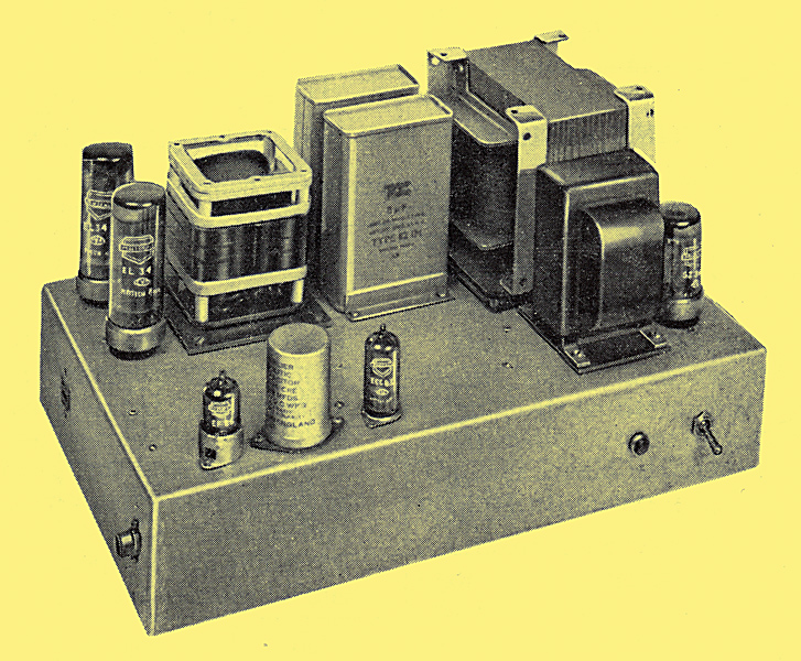
The completed prototype amplifier
The circuit to be described is designed to give the highest standard of sound reproduction when used in association with a suitable pre-amplifier, a high-grade pick-up head and a good-quality loudspeaker system.
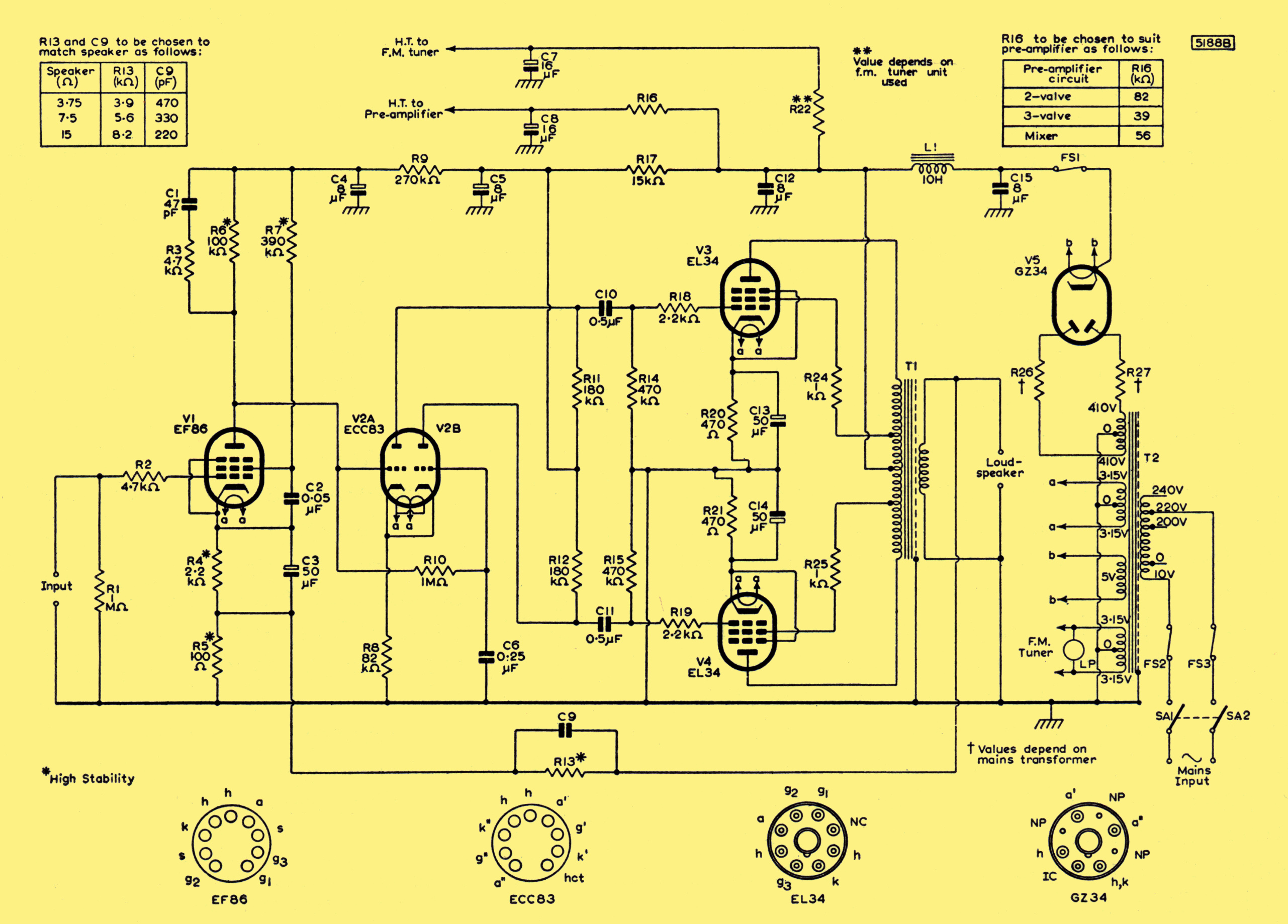
Two Mullard output pentodes, type EL34, rated at 25W anode dissipation, form the output stage of the circuit. These are connected in a push-pull arrangement with distributed loading, and give a reserve of output power of 20W with a level of harmonic distortion less than 0.05 %. The intermediate stage consists of a cathode-coupled, phase-splitting amplifier using the Mullard double triode, type ECC83. This stage is preceded by a high-gain voltage amplifier incorporating the Mullard low-noise pentode, type EF86. Direct coupling is used between the voltage amplifier and phase splitter to minimise low-frequency phase shifts.
The main feedback loop includes the whole circuit the feedback voltage being derived from the secondary it winding of the output transformer and being injected it in the cathode circuit of the EF86. The amount of feedback applied around the circuit is 30dB, but in spite of this high level, the stability of the circuit is good and the sensitivity is 220 mV for the rated output power. The level of hum and noise is 89dB below the rated 20W.
The rectifier used in the power-supply stage is the Mullard full-wave rectifier, type GZ34. This provides sufficient current for the amplifier (about 145 mA) and also for the pre-amplifier and FM radio tuner unit (about 35 mA) being used with it.
Circuit Description
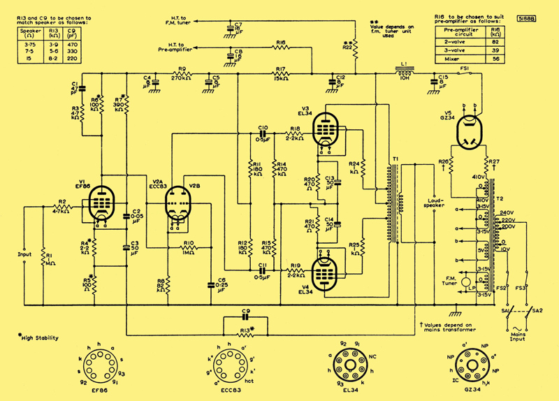
The full circuit. A hi-resolution jpg can be accessed by clicking the image
Input Stage
The EF86 input stage of the circuit above provides high-gain voltage amplification, the stage gain being approximately 120 times. High-stability, cracked-carbon resistors are used in the anode, screen-grid and cathode circuits, and they give an appreciable improvement in the measured level of background noise compared with ordinary carbon resistors.
The stage is coupled directly to the input of the phase splitter. The purpose of this is to minimise low-frequency phase shift in the amplifier and to improve the low-frequency stability when negative feedback is applied. A CR network (C1, R3) connected across the anode load produces an advance in phase and thus improves the high-frequency stability of the amplifier.
Intermediate Stage
The second stage of the circuit uses a Mullard double triode, type ECC83, and fulfils the combined function of phase splitter and driver amplifier. The phase splitter is a cathode-coupled circuit which enables a high degree of balance to be obtained in the push-pull drive signal applied to the output stage.
With the high line voltage available, the required drive voltage for an output power of 20 W is obtained with a low level (0.4 %) of distortion. The anode load resistors R11 and R12 should be matched to within 5%, R12 having the higher value for optimum operation. Optimum balance is obtained when the effective anode loads differ by 3 %. The grid resistors R14 and R15 of the output stage should also be close-tolerance components because they also form part of the anode load of the driver stage. High-frequency balance will be determined largely by the wiring layout because equality of shunt capacitances is required. Low-frequency balance is controlled by the time constant C6 R10 in the grid circuits of the triode sections, and the value chosen will give adequate balance down to very low frequencies.
A disadvantage of the cathode-coupled form of phase splitter is that the effective voltage gain is about half that attainable with one section of the valve used as a normal voltage amplifier. However, as the amplification factor of the ECC83 is high (100), the effective gain of the cathode-coupled circuit is still about 25 times.
Output Stage
The main feature of interest in the output stage is the use of two EL34 with partial screen-grid (or distributed) loading, the screen grids being fed from tappings on the primary winding of the output transformer. The best practical operating conditions are achieved with this type of output stage when about 20 % of the primary winding is common to the anode and screen-grid circuit.
The anode-to-anode loading of the output stage is 7k Ohms and, with a line voltage of 440 V at the centre-tap of the primary winding of the output transformer, the combined anode and screen-grid dissipation of the output valves is 28W per valve. With the particular screen-grid to anode load ratio used, it has been found that improved linearity is obtained at power levels above 15 W when resistors of the order of 1,000 Ohms are inserted in the screen-grid supply circuits. The slight reduction in peak power-handling capacity which results is not significant in practice.
Separate cathode-biasing resistors are used in the output stage to limit the out-of-balance direct current in the primary winding of the output transformer. The use of other balancing arrangements has not been thought necessary although it is likely that some improvement in performance, particularly at low frequencies, would result from the use of DC balancing. It is necessary in this type of output stage for the cathodes to be bypassed to earth even if a shared cathode resistor is used. Consequently, a low-frequency time constant in the cathode circuit cannot be eliminated when automatic biasing is used.
Negative Feedback
Negative feedback is taken from the secondary winding of the output transformer to the cathode circuit of the input stage. In spite of the high level of feedback used (30 dB), the circuit is completely stable under open-circuit conditions. At least 10 dB more feedback (obtainable by reducing the value of R13) would be required to cause high-frequency instability. The most probable form of instability would be oscillation with capacitive loads, but this is most unlikely to occur even with very long loudspeaker leads.
Power Supply
The power supply is conventional and uses a Mullard indirectly-heated, full-wave rectifier, type GZ34, in conjunction with a capacitive input filter. The values of the limiting resistors R26 and R27 will depend on the winding resistances of the mains transformer used. Their purpose, when required, is normally one of voltage control only. Where a transformer with a very low winding resistance is used, a secondary voltage rated at 400-0-400V may be found adequate. The rating of the mains transformer is such that about 40 mA may be drawn from the HT supply to feed a pre-amplifier circuit and FM tuner in addition to the normal current required (about l45 mA) for the amplifier.
Extra decoupling will be needed for these ancillary supplies. The smoothing component R22 can only be chosen when the type of tuner to be used is known. A value of about 6k Ohms. would be suitable for typical current and voltage requirements of approximately 35 mA and 200 V. The components R16 and C8 depend on the pre-amplifier to be used. The values given in the circuit diagram refer to the 2- and 3-valve pre-amplifiers and the mixer unit described in our publications.
Construction and Assembly
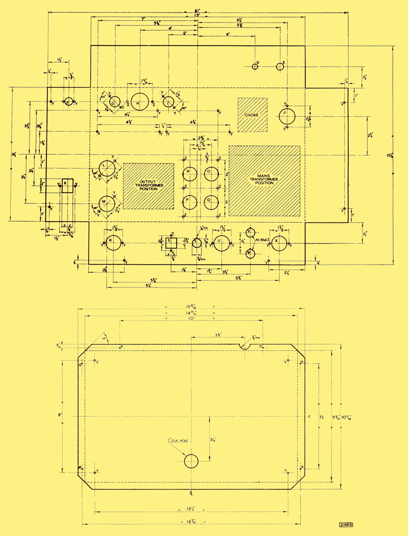
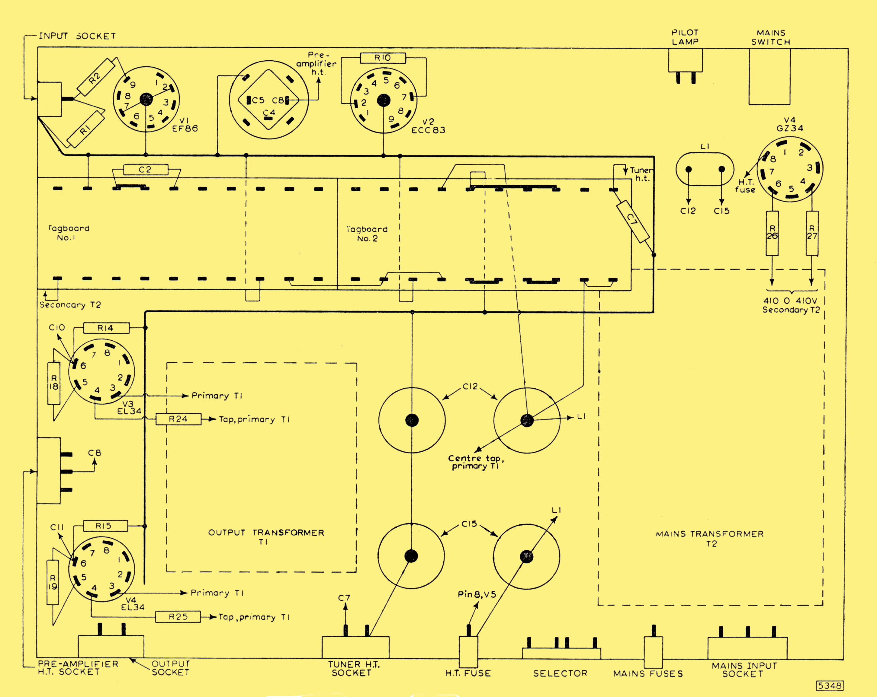
Chassis and base marking-out diagram
The chassis for the 20 W amplifier are made from two separate pieces of 16 SWG brass or steel sheet. The dimensions (in inches) of these pieces are:
(a) Main chassis 21 x 15.5
(b) Base 15.91 x l0.41
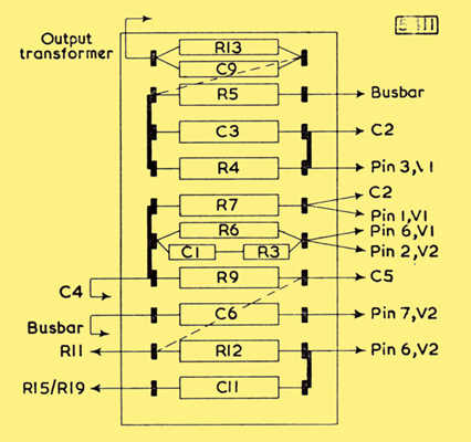 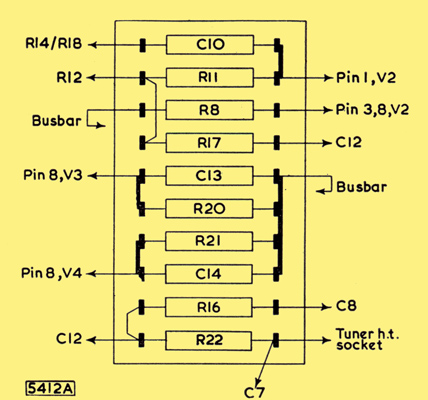
Tag-board one and tag-board two
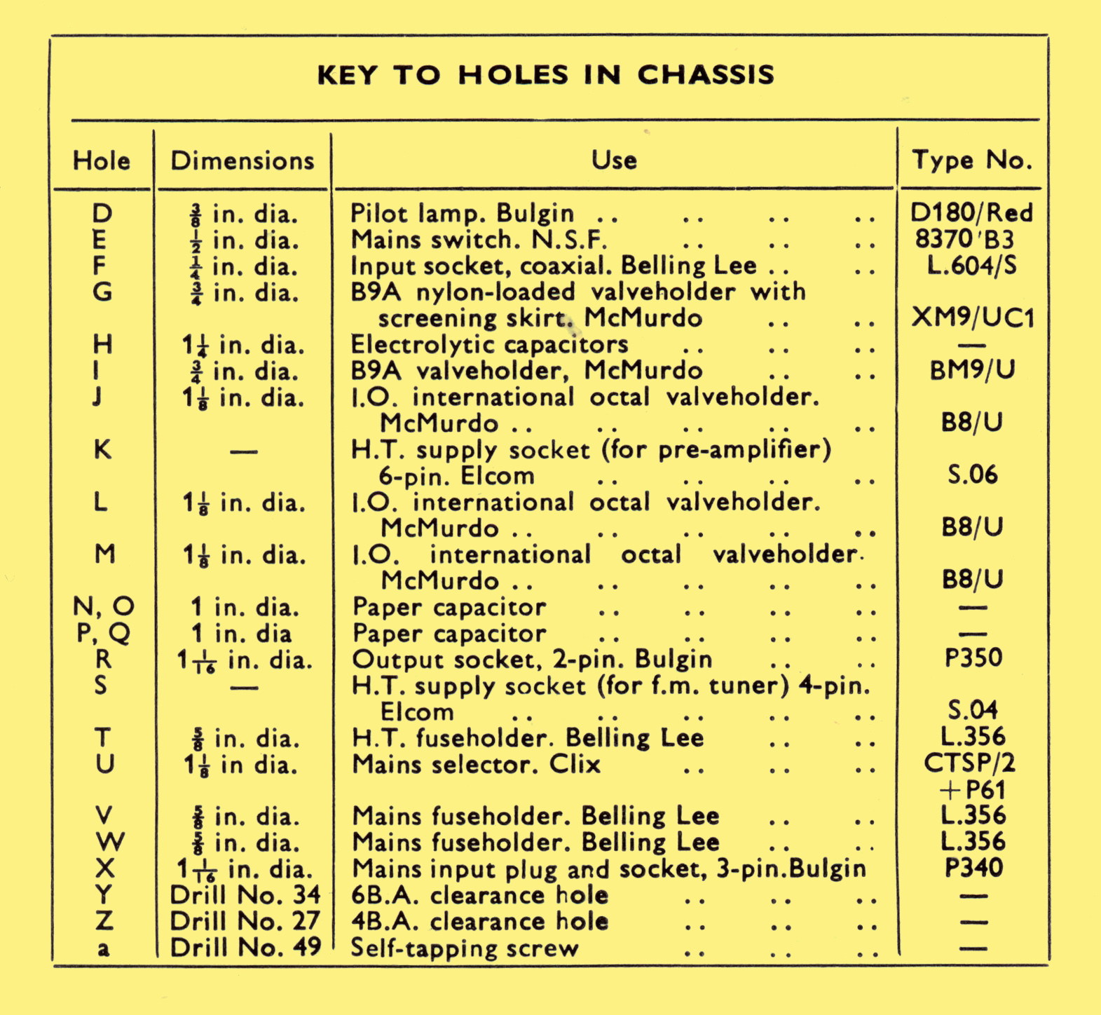
Each piece should be marked as shown in the drawings above and the holes should be cut as indicated in the table below. Where bending is required, it is important for the bends to be made accurately at the lines for the pieces to fit together properly on assembly. Most of the resistors and small capacitors are mounted on two ten-way tag-boards, and they should be connected as indicated above. The larger components should be fitted to the chassis in the positions indicated in the layout diagram below this arrangement of the components will ensure good stability.
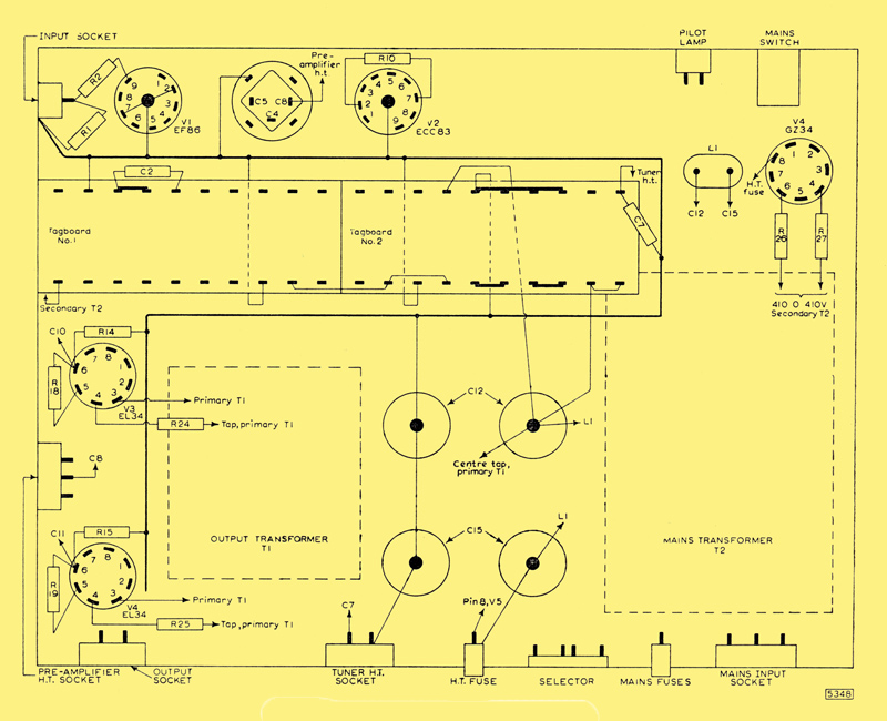
Suggested component layout
The wiring between the components is also indicated in the above diagram. A busbar earth return is indicated, with only a single chassis connection at the input socket. Of the valve holders fitted to the chassis, only the holder for the EF86 needs to be skirted. This holder should also be nylon-loaded.

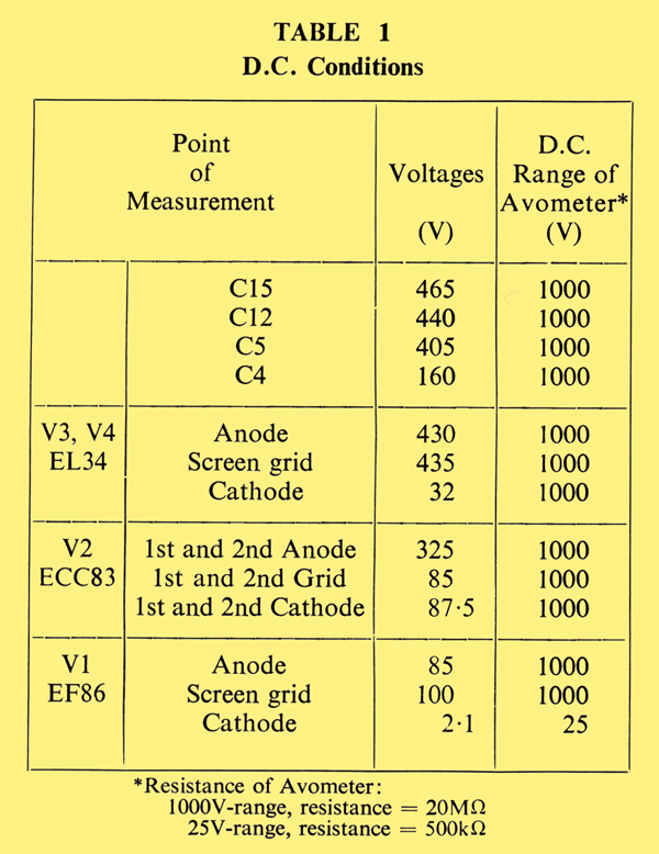
DC Conditions
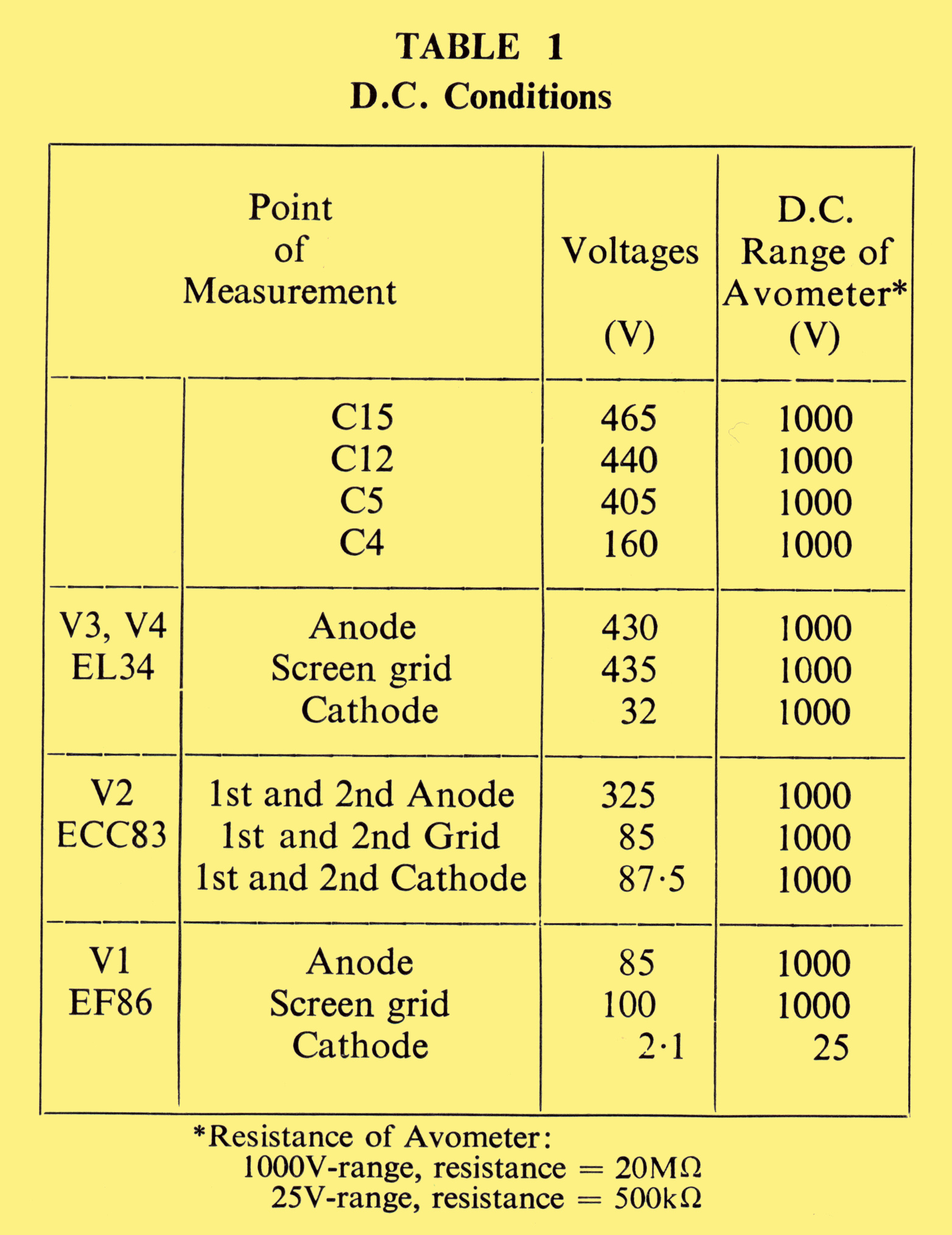
The DC voltages at points in the equipment should be tested with reference to table 1 above. The results shown in this table were obtained with an Avometer No.8. (20,000 ohms per volt).
Performance
Distortion
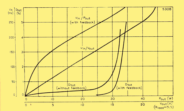
Harmonic distorting and output/input characteristics
The total harmonic distortion of the prototype amplifier at 400 Hz, measured without feedback and with a resistive load, is shown above. The distortion curve towards the overload point when feedback is applied is also shown in the diagram above. At the full rated output, the distortion without feedback is well below 1 % and with feedback is below 0.05 %. The distortion rises to 0.1 % for an output power of 27 W. The loop-gain characteristic is such that a level of at least 20 dB of feedback is maintained from 15 Hz to 25 Hz, and of at least 26 dB down to 30 Hz.
Measurements of intermodulation products were made in the prototype amplifier using a carrier frequency of 10k Hz and a modulating frequency of 40 Hz. The ratio of modulating amplitude to carrier amplitude was 4 : 1. With the combined peak amplitudes of the mixed output at a level equivalent to the peak sine-wave amplitude at an RMS power of 20 W, the intermodulation products, expressed in RMS terms, totalled 0.7 % of the carrier amplitude. At an equivalent power of 27 W, the products totalled 1 % of the carrier amplitude. The beat-note distortion between equal-amplitude signals at frequencies of 14 and 15k Hz is 0.25 and 0.3 % at equivalent powers of 20 and 27 W respectively, and between frequencies of 9 and 10k Hz it is 0.2 and 0.25 % at the same equivalent powers. The variations of intermodulation and beat-note distortion with equivalent power are plotted in the diagram below.
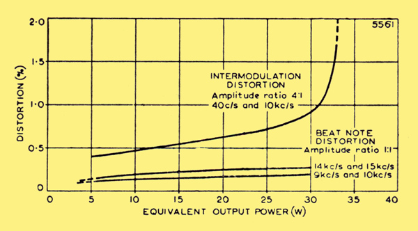
Intermodulation and 'beat note' distortion
The output/input characteristics of the prototype amplifier are shown above. Excellent linearity is indicated up to output voltages, measured across a 150 load, of 20 V, which corresponds to an output power of 27 W.
Frequency Response
Frequency response, loop-gain and phase shift characteristics
c/s or cycles per second is the old frequency unit. Hz or Hertz the modern unit. Hz is used in the text.
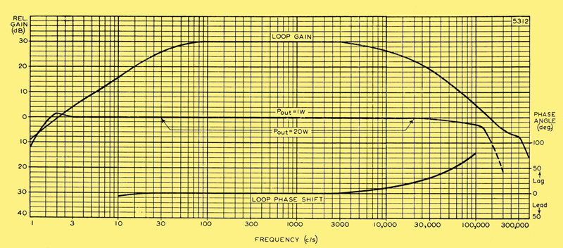
The frequency- and power-response characteristics that is, the curves for output powers of 1 and 20 W respectively-are shown above. From this figure it will be seen that, at an output of 1 W, the characteristic is flat (±1 dB) compared with the level at 1k Hz from 2k Hz to 100k Hz and the power-respons characteristic is flat (±0.5 dB) from 3O Hz to 20k Hz. It is important that adequate power-handling capacity is available at the low-frequency end of the audible range and this is determined chiefly by the characteristics of the output transformer. The prototype amplifier is capable of handling powers of at least 20 W at frequencies as low as 30 Hz without excessive distortion, but for very low frequencies it is desirable that the signal should be attenuated in the associated preamplifier .
Sensitivity
The sensitivity of the amplifier measured at 1k Hz is 6.5 mV for an output of 20 W when no feedback is applied, and approximately 220 mV with feedback, the loop gain being 3O dB. The loop-gain characteristic of the complete amplifier for the full frequency range is shown above. The sensitivity, with feedback, at the overload point (27 W) is approximately 26O mV.
The level of background noise and hum in the prototype equipment is 89 dB below 20 W, measured with a source resistance of lOk Ohms. This is equivalent to a signal of about 5.5μV at the input terminals. It is possible to increase the overall sensitivity of the amplifier by 6 dB while still maintaining a low background level, a high loop gain and a good margin of stability, but various design requirements of associated pre-amplifier circuits (the need for a high signal-to-noise ratio, for example) render a higher sensitivity a doubtful advantage.
Phase Shift and Transient Response
Emphasis has been laid in the amplifier on a good margin of stability and, consequently, the phase shift is held to a comparatively low level. As shown above, the shift is only 200 at 20k Hz. Excellent response to transient signals is obtained, the rise time of the amplifier being of the order of 5μSec.
Output Impedance
The output stage has a low inherent output impedance, and this is further lowered by the use of negative feedback. It is approximately 0.3 Ohms with a 15 Ohm load for an output of 20 W at frequencies of 4O Hz, lk Hz and 20k Hz. This gives a damping factor of about 50.
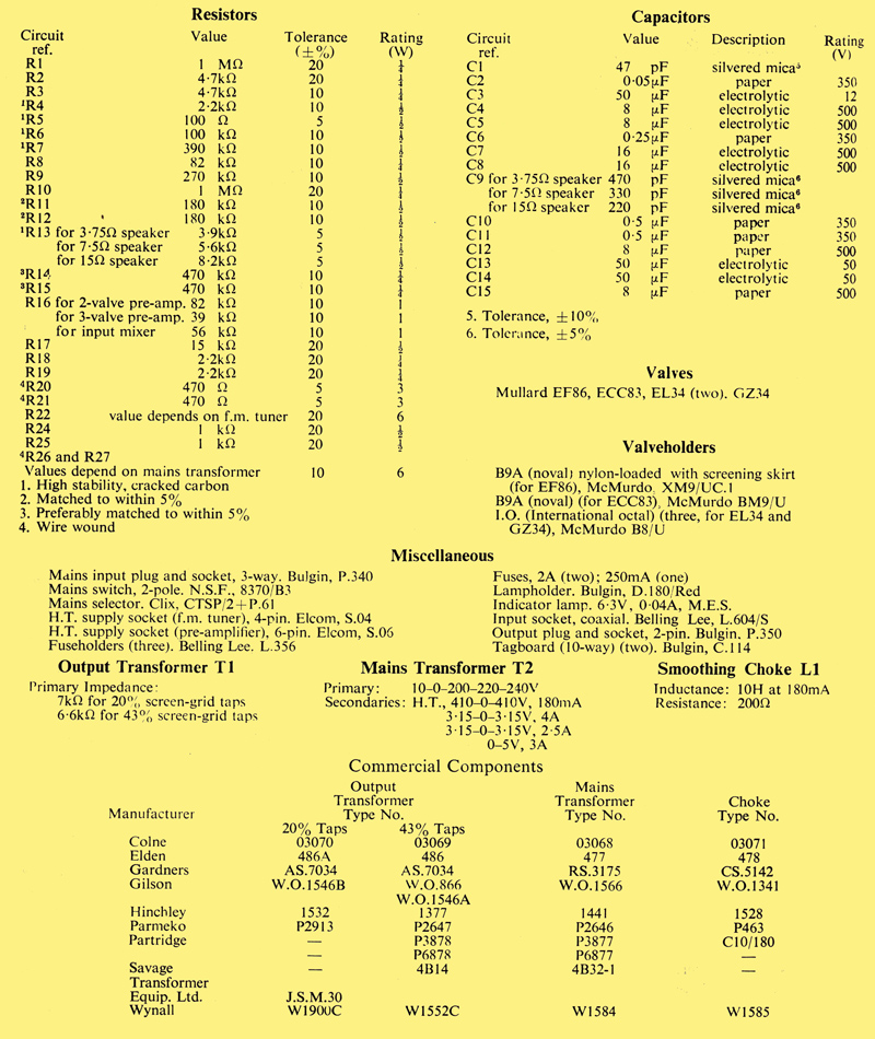
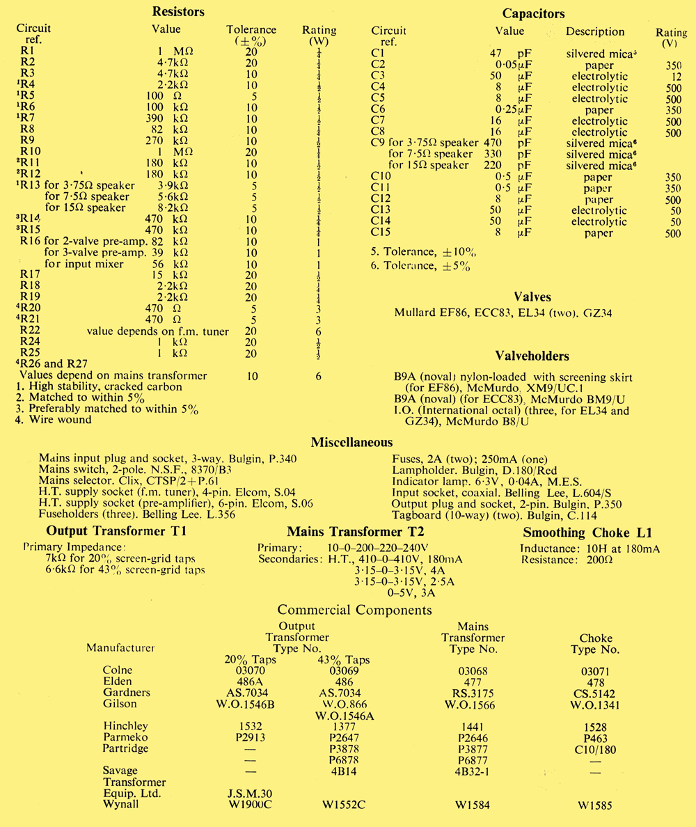
Full components list of the 1950's prototype
|