|
Phase Splitter Circuits
Last time we commenced an examination of valve phase-splitter circuits suitable for providing out-of-phase AF voltages for application to the control grids of two output valves in push-pull. We then examined the split-load phase-splitter, this consisting of a single triode having equal values of resistance in its anode and cathode circuits. The out-of-phase voltages then appear at the anode and cathode of the triode.
We now carry on to further types of phase-splitter.
The Paraphase Amplifier
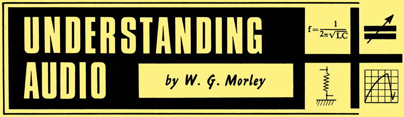
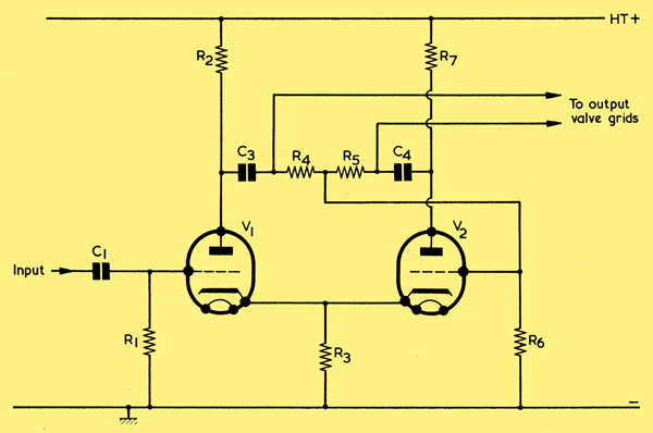
The paraphase amplifier phase-splitter. V2 provides the requisite phase reversal.
A very simple phase-splitter circuit is illustrated above. In this diagram the input AF signal is applied, by way of C1 and grid resistor R1, to V1, which functions as a normal voltage amplifier. An amplified version of the input signal appears at the anode of V1, R2 being the anode load. The anode signal from V1 is fed, via C3, to the potentiometer given by R4 and R5, the signal voltage at the junction of these two resistors being passed . to the grid of V2. V2 is similar to V1, and the two triodes could consist, in practice, of a double-triode valve. V1 anode load, R2, is equal in value to R6. Similarly, cathode resistor R3 is equal in value to R7. C2 and C4 are electrolytic cathode bypass capacitors, and C1, C3 and C5 are AF coupling capacitors.
The signals for the control grids of the following push-pull stage are taken from the anodes of V1 and V2 via C3 and C5 respectively. The output via C3 is merely the input signal amplified by V1 whilst the output via C5 is the same signal after further amplification by V2. V2 provides 180° phase reversal, with the result that the two signals are 180° out of phase, as is required of the circuit.
The input signal to V2 grid is attenuated by R4 and R5, the attenuation being such that the output via C5 is equal in amplitude to the output via C3, as is also required of the circuit. To see how the desired amount of attenuation is achieved, let us assume that V2 offers a voltage gain of 40. R4 and R5 are then given values which ensure that 1/40 of the signal voltage from C8 is passed to V2 grid. In general, (R4+R5)/R5 should be equal to the voltage gain of V2.
R4 plus R5 are equal to R8, and it will be noted that R4 plus R5 can be used as the grid resistor for one of the push-pull output valves whilst R8 can be used as the grid resistor for the other push-pull output valve. Each output voltage is an amplified version of the input voltage, the amplification being that provided by V1.
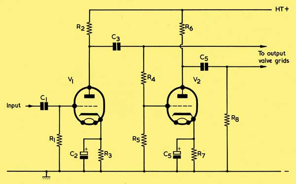
(a) The separate cathode resistors and bypass capacitors in the first illustration may be replaced by a single cathode resistor and bypass capacitor, as shown here
(b) The bypass capacitor may also be omitted, and a single cathode resistor employed on its own
(c) For convenience of adjustment, R4 and R5 can be replaced by a preset potentiometer. A fixed resistor inserted at the point marked with a cross could be added to limit the range offered by the potentiometer and make its setting-up easier to carry out.
The cathodes of V1 and V2 may share a common cathode resistor and bypass capacitor, as in (a) above. The single resistor should have half the value of either R5 or R7 in the top image on the page, since it is required to drop the same cathode bias voltage at twice the current. Since the AF currents passed by the cathodes of V1 and V2 are assumed to be equal and opposite, the bypass capacitor may be dispensed with, as in (b). In. practice, however, omitting the common cathode bypass capacitor may result in some unbalance at extreme high and low frequencies.
An advantage of the phase-splitter circuit under discussion is that both the triode cathodes couple to chassis via a low value resistor, with the result that there is less likelihood of hum pick-up from the heater supply than with the split-load phase-splitter we discussed in the previous article. On the other hand the circuit suffers from the disadvantage that, for good balance, R4 and R5 have to be adjusted to cater for the actual voltage gain provided by V2. Thus, R4 and R5 may need to be altered if a new valve is fitted in the V2 position or if the voltage gain offered by the existing valve varies as it ages. The changes in value could be conveniently made, incidentally, by replacing R4 and R5 by a preset potentiometer, as in (c). A further disadvantage is that the output signal obtained from V2 has undergone an extra stage of amplification, and may in consequence be a slightly distorted version of that obtained from V1. Also, the signal obtained from V2 passes through an extra capacitor, C5, whereupon some unbalance at the lower audio frequencies, where the reactance of C5 becomes appreciable, may occur. This last point can be of importance in high quality or high fidelity applications.
The phase-splitter shown at the top of the article is sometimes described as a paraphase amplifier. However, the world paraphase tends to be applied to other amplifying circuits which offer two push-pull outputs for a single input, and this fact should be borne in mind when references to the term are encountered.
See-Saw Phase Inverter
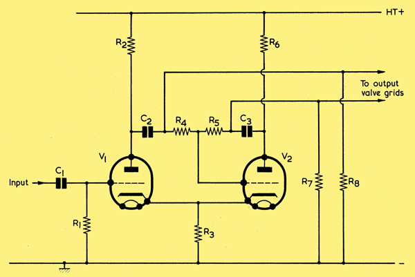
The see saw phase inverter. In this circuit R4, R5 and R6 are closely matched in value.
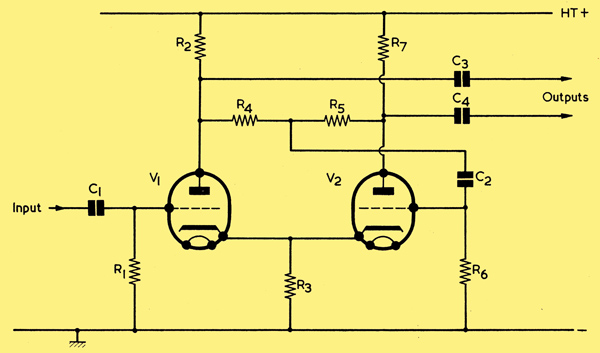
The diagram shows a phase-splitter circuit which is known as a see-saw phase inverter. For the circuit to function correctly, R4, R5 and R6 are closely matched in value, which can be typically 1MΩ. Also, capacitor C2 should have negligible reactance at the audio frequencies it is intended to handle. R2 and R7 are merely anode load resistors. Both have the same value, which is that normally employed by either triode when used as a voltage amplifier. The two cathodes of the double-triode are connected together and couple to chassis via cathode bias resistor R3. As we shall see shortly, there is no necessity for a cathode bypass capacitor. Capacitors C1, C3 and C4 are AF coupling capacitors, and R1 is the grid resistor for V1. The two outputs provide out-of-phase signals for the grids of a following push-pull output stage.
When an AF input is applied to the grid of V1 an amplified signal appears at its anode. Ignoring the action of V2 for the moment, this signal is applied to the potentiometer given by R4 and R6 (C2 has negligible reactance) and a portion is applied to the grid of V2. Thus, the grid of V2 has applied to it a signal of the same phase as that at the anode of V1. V2, whose action we have ignored up to now, amplifies this signal and an amplified version, 180° out of phase with that at V1 anode, appears at the right-hand end of R5. In consequence, when the operation of V2 is considered we find that amplified signals of opposite phase appear at the outside ends of R4 and R5, the signal at their junction being fed to the grid of V2.
Because the values of R4, R5 and R6 are equal, the circuit has an automatic tendency to give output signals of nearly equal voltage amplitude. If, for some reason, the amplitude of the signal at the anode of V2 were to decrease, the signal at the junction of R4 and R5 would contain a higher proportion of the V1 anode signal. This higher proportion would be applied to the grid of V2, resulting in an increase in signal amplitude at V2 anode which would counteract the previous decrease. Put another way, the circuit stabilises because the amplitudes of the signals at V2 anode and grid are interdependent; the anode signal amplitude must always be that which causes the corresponding signal amplitude to appear at the grid. The equilibrium taken up by the circuit is such that the signal at the junction of R4 and R5 always contains a small proportion of the signal at the anode of V1. To obtain output voltages in practice which are closely equal in amplitude, R4, R5 and R6 should be components having a tolerance of ±5% or better, selecting R5 to have a slightly higher value that R4. Also V2 should be a type offering a high degree of voltage amplification.
A slight rearrangement of the previous circuit gives this floating paraphase phase-splitter, in which C2 is not required. Some floating paraphase phase-splitters have separate cathode bias resistors, with parallel bypass capacitors, for the two triodes.
The see-saw phase inverter provides amplification, this being given by V1. Each output has very nearly the same amplitude as would appear at the anode of V1 if this triode operated on its own as a normal voltage amplifier. Both output impedances are the same, and the two outputs in the diagram above may connect direct to the push-pull output grids. Also, the valve cathodes connect to chassis via a low-value resistor, with the result that hum pick-up from the heater supply is liable to be low. R3 has a value equal to half that of a normal cathode bias resistor for either triode on its own. There is no necessity to connect a bypass capacitor across R3 because it carries both anode currents, these being opposite in phase and (very nearly) equal. The phase splitter derives its name from the fact that the outer ends of R4 and R5 swing in the manner of the ends of a see-saw about a fulcrum, the latter being slightly to the right of their junction. V1 and V2 may, in practice, consist of a double-triode valve.
There are a number of phase splitter circuits which operate in a similar manner to that of the see-saw circuit. These can all be identified by the fact that they have two valves whose anodes feed into the distinctive pattern of three closely matched resistors (with the junction coupling to the grid of the second valve) given in the see-saw circuit by R4, R5 and R6. In some versions R4 and R5 may be grid resistors for the push-pull output valves, the anodes being coupled to them via coupling capacitors as shown above. Such circuits are generally described as floating para-phase phase splitters, the term floating deriving from the fact that the grid of the second valve is connected to a floating point in the circuit. As was mentioned earlier, the term paraphase applies. to an amplifier which converts a single input into two push-pull outputs. If, with the see-saw circuit, C2 presents appreciable reactance at the lower audio frequencies, some unbalance at such frequencies is possible. Unbalance of this nature is less liable to occur with the somewhat more symmetrical second circuit, where both anodes couple into R4 and R5 by way of coupling capacitors C5 and C4, these having equal values.
A development of the circuits of the first two circuits is given below. In this circuit there are only two closely matched resistors, R4 and R5. These resistors may similarly be of the order of 1MΩ in value. R2 and R6 are normal anode load resistors having equal values, whilst C2 and C3 are equal value AF coupling capacitors. The same self-balancing action occurs as with the previous circuits, the signal at the anode of V2 having an amplitude which causes the corresponding signal amplitude to be applied to its grid. This circuit provides slightly better balance than do those presented earlier. It will be seen that the grid of V2 is maintained at chassis potential so far as bias is concerned by way of R4, R5, R7 and R8. R7 and R8 are the grid resistors for the output valves.
In the three circuits just discussed balance improves, in all cases, as the voltage gain offered by V2 increases. In consequence it is desirable to use a high gain valve here, and a suitable choice would be one section of an ECC83 double-triode. The other section of this valve can then be employed as V1.
A development from the circuits above. Only two closely matched resistors, R4 and R5, are required here.
Next we shall complete our examination of phase-splitters by discussing the Schmitt phase inverter, after which we shall introduce the subject of negative feedback.
|