|
A common reaction, when considering a stabilised power supply employing either valves or transistors, is to think in terms of the series circuit. But the shunt stabiliser can offer similar performance and can, in many cases, be cheaper than a series stabiliser. Our contributor devotes most of this article to the shunt circuit as applicable to valve power supplies. Mathematical analyses are given to support the description of operation, and it is shown that the end results of the calculations are simple equations which can be readily applied.
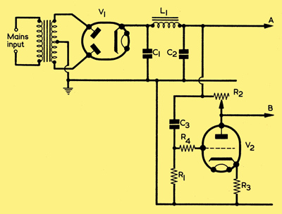
An electronic smoothing circuit
Voltage stabilisers using thermionic tubes can be divided into two main types, namely series and shunt stabilisers. In series stabilisers all of the stabilised current passes through a series valve, the potential drop across this valve being controlled by the applied grid potential. Several valves are usually required in this type of circuit. In shunt stabilisers, the controlling valve appears across the power supply output.
Shunt valve stabilisers will be considered in some detail since they are simple and some types can be constructed using only a single valve.
Electronic Smoothing
If a power supply circuit is required which will provide an output that is almost completely free from hum or other ripple, the type of circuit shown above may be used. This circuit will also remove any hum harmonics and any transient voltage pulses which may be present in the mains supply due to random changes in the loading. The smoothed output is taken from point B and should be used to supply only the circuits which really do need a well smoothed supply. All other parts of the equipment should be fed from point A. in order to ensure that the current passing through resistor R2 is kept as small as possible.
Principle of Operation
If the potential across C2 increases slightly for any reason (for example, during a peak of the hum derived from the mains supply), this voltage peak will be applied to the grid of the valve V2 via capacitor C3. The anode current passing through the valve thus increases and this tends to reduce the voltage at point B due to the increased voltage drop in R2.
If the component values are suitably chosen, the increased voltage drop across R2 can be made equal to the initial rise in potential, so that the potential at point B remains constant. One can think of the valve as being a phase inverter producing an output of opposite polarity to the instantaneous voltage and (in this circuit) having a gain of unity. All of the alternating current (due to hum, etc.) passing through R2 also passes through the valve. The resistor R4 serves to protect the valve against excessive grid current during any positive voltage transients of the potential at point A.
This circuit has an input time constant of approximately C3R1 and will be effective at frequencies greater than approximately 1/C3R1.
Circuit Analysis
The resistor R3 provides a suitable bias for the valve. The value of this resistor may be calculated from the equation:-
R3 = Vg/Ia . . . . Equation 1
where Vg is the grid bias recommended by the valve manufacturers and Ia is the anode current at this bias. This sets the DC conditions.
The value of R2 may be found from a consideration of the AC circuit conditions; it must be chosen so that the gain of the stage is unity. Let the AC input voltage applied between the grid and earth be Vin; The grid-to- cathode AC voltage, Vgc, is given by the equation:-
Vin = Vgc + VR3 . . . . Equation 2
Where VR3 is the alternating potential across R3. As far as alternating voltages and currents are concerned, the circuit may be represented by the constant voltage equivalent as below.
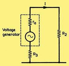
Equivalent circuit for the V2 stage in the circuit above.
The components inside the dotted lines are equivalent to the valve. The valve effectively generates an alternating potential of -μVgc Volts where μ is the amplification factor of the valve. The minus sign, which indicates that the output voltage is 180° out of phase with the input voltage, will be ignored in the following calculation.
The current flowing, I, is given by Ohms Law as:-
I = μVgc/(R2 + R3 + ra)
The alternating voltage across R2 is IR2, so:-
VR2 = μVgc(R2 + R3 + ra)R2
Similarly, the alternating voltage across R3 is given by:-
VR3 = μVgc(R2 + R3 + ra)R3
In order that the gain of the stage shall be unity, the value of the output voltage, VR2, must satisfy the equation:-
VR2 = Vgc + VR3 (see equation 2)
That is:-
μVgc(R2 + R3 + ra)R2 = Vgc + μVgc(R2 + R3 + ra)R3
Dividing through by Vgc and multiplying by (r2 + R3 + ra), we obtain:-
μR2 = R2 + R3 + ra + μR3
∴ μ - 1)R2 = ra + (μ + 1)R3
Hence, R2 = ra/(&mu - 1) + (μ + 1)/(μ - 1)R3
As μ is much greater than unity, μ - 1 and μ + 1 are both approximately equal to μ, thus:-
R2 ≈ ra/μ + R3
or R2 ≈ 1/gm + R3 (since μ = gm x ra . . . . Equation 3
In practice it is best to employ a variable resistor for R2 and to adjust it until no hum is detectable at point B. For hum detection this point may be connected via a DC blocking capacitor to the input of a - sensitive audio amplifier or to the input of an oscilloscope.
The capacitor C3 must be a good quality paper component; an electrolytic capacitor is quite unsuitable owing to the fairly high leakage. The resistor R1 provides a DC path between the grid and cathode of the valve and should not have a value above the maximum specified by the valve manufacturer.
Practical Example
Let us design a circuit using half of an ECC81 (12AT7) double triode in the circuit. The recommended grid bias voltage is -2.0 Volts and the resulting anode current about 10 mA. Hence:-
R3 = 2.0/10 x 10-3 = 200Ω using equation 1
From valve data, gm for the ECC81 is 5.5 mA/Volt. Using equation 3:-
R2 ≈ 1/gm + R3 ≈ 1/(5.5 x 10-3+ + 200 ≈ 182 + 200 ≈ 382Ω
Hence a 500Ω variable resistor would be suitable for use as R2. R4 may bc about 50kΩ to 100kΩ. In the case of the ECC81, the maximum permissible resistance between grid and cathode when cathode bias is employed is 1MΩ. R3 and R4 are fairly small compared with this and therefore R1 may be 1MΩ. The capacitor C3 should be large if slow variations of the mains supply voltage are to be smoothed out. For most purposes, however, a 0.1μF paper capacitor is suitable for this position, since it will only be necessary to eliminate hum.
Stabilisation
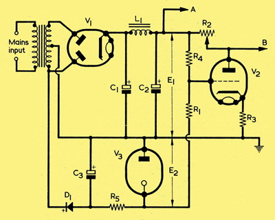
A shunt stabiliser circuit
The circuit we have been considering will provide smoothing but not stabilisation, since capacitor C3 will not pass zero frequency variations of potential to the grid of the valve. The type of circuit shown immediately above will provide both stabilisation and smoothing, but requires a negative stabilised HT supply in addition to the HT supply being smoothed. However, the negative HT current required is quite small and may be obtained by the method shown in the circuit. D1 is a small power rectifier diode of suitable peak inverse voltage rating (not less than 2√2 times the RMS transformer secondary voltage). C3 is the negative HT supply reservoir capacitor and V3 is a gas filled voltage stabiliser tube such as the 90C1 which has a working voltage of, very approximately, 100 Volts. The resistor R5 is used to drop the voltage across C3 to the voltage stabiliser operating voltage; if it is omitted, the voltage stabiliser will be damaged.
The coupling to the grid of V2 is via resistors in order that the circuit is effective for very slow changes of the mains supply voltage. R1 should not exceed the maximum grid-to-cathode resistance recommended by the manufacturers for valve V2. R4 is selected so that the ratio R4/R1 is approximately equal to the ratio of the steady potentials E1/E2. The mean grid potential of V2 is then approximately equal to the earth potential. R3 is calculated as in the previous circuit to provide a suitable bias voltage for V2.
Calculation of R2
The value of resistor R2 may be calculated in a similar way to the value of the corresponding resistor in the first circuit. In the case of our new circuit, however, the value of the alternating potential between the grid and earth is less than the alternating voltage across the capacitor C2, since the resistors R4 and R1 act as a potential divider to the AC component as well as the DC component. To take this into account, the value of R2 has to be multiplied by the factor (R1 + R2)/R1 or, since V2 grid is virtually at earth potential, (E2 + E1)/E2.
This in our new circuit,
R2 ≈ ((1/gm) + R3)(1 + (E1/E2))
This equation enables the approximate value of R2 to be found, but it is best to employ a variable resistor of a value somewhat higher than is given by the equation so that it can be adjusted for optimum stabilisation and hum removal.
It remains to find the value of R5. First of all the current passing through R1 must be found. This is equal to E1 + E2 divided by R4 + R1. The current through the stabiliser V3 should be selected to be in the working range of this tube. For example, the 90Cl has a working current range of 1 to 40 mA, so a current of 10 mA may be selected. The total current passing through R5 is the sum of this current and that passing through R1. The value of the potential across R5 is equal to the potential across C3 minus the working potential of the tube V3. The value of R5 should be approximately equal to the voltage across it divided by the calculated total current passing through it. (The potential across capacitor C3 will be somewhat less than √2 times the RMS voltage of half the transformer secondary winding.)
C1, C2, C3 and L1 of this circuit and C1, C2 and L1 of the first circuit are normal smoothing components, typical values for the capacitors being 8 or 16μF and for the inductors 5 or 10 Henrys.
Feedback Shunt Stabilisers
The circuits which have been discussed so far are bridge type stabiliser and smoothing circuits in which hum voltages, etc., may be entirely eliminated by the use of a valve as a part of a balanced bridge.
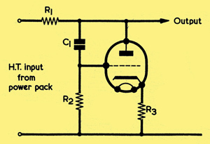
A feedback shunt smoothing circuit
Another type of electronic smoothing circuit is shown above. Although this circuit does not, at at least at first sight, appear very much different from those described previously, the principle of operation is rather different. In particular it should be noted that the grid is coupled to the anode of the valve and not to the input from the power pack. Thus the circuit cannot entirely eliminate mains voltage variations, since only the variations of the output are coupled to the grid. This type of feedback stabiliser circuit has, however, the compensating advantage that the output impedance is usually lower than that of the bridge circuits discussed so far. Thus, this circuit is likely to be most suitable when changes of loading are expected to occur.
An analysis of the circuit will show that this circuit will reduce the amount of hum by the factor:-
1 + gm(R1RL) / (r1 + RL)(1 / (1 + gmR3)
where RL is the resistance of the load. Hence the mutual conductance, gm, of the valve should be large, whilst R3 should be kept as small as possible.
The output resistance effectively connected across the load is approximately the resistance R1 connected in parallel with the output resistance of the valve in series with R3. As in the case of the cathode follower, 100%, negative feedback is used and therefore the output impedance of the valve alone is approximately 1/gm, as with the cathode follower. Thus the output impedance, R, is given by the approximate equation:-
1/R = 1/R1 + 1/(1/gm + R3)
In order to keep the output impedance, R, small, gm should therefore be large and R3 small. This is the same condition as is required to obtain the best rejection of hum.
If C1 is replaced by a resistor, a stabilising circuit is obtained which will operate at any frequency (including zero frequency), instead of having the lowest operating frequency limited by the time constant of C1R2. It is best to bypass the anode to grid resistor by a capacitor, however, since 100% negative feedback is then obtained at hum frequencies and the output impedance at such frequencies is also kept to a minimum.
Although only single valve shunt stabilisers have been discussed in this article, various circuits have appeared in the literature which employ several valves. These enable the hum or slow variations in the HT potential to be completely eliminated and may be designed so that the output impedance is very low or even zero in certain cases.
Series Stabilisers
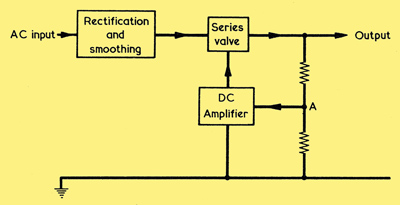
Block diagram for a series stabiliser.
The next block diagram may be used to illustrate the functioning of a series stabiliser. All of the output current from the rectification and smoothing circuit passes through a series stabiliser valve to the output. The potential drop across this valve is dependent on its grid voltage, which is controlled by the output potential, The fraction of the output voltage tapped off by the potential divider at point A is amplified by the DC amplifier and used to control the grid voltage of the series valve. It is not possible to entirely eliminate output fluctuations with this type of feedback circuit, since the DC amplifier will only operate when small variations of the output occur.
The series valve should have a low internal anode resistance, ra. The gm should be fairly high if a high degree of control is required. A power output valve is almost invariably used, since an appreciable current will probably have to be passed. (If the current requirements are small, the shunt circuits so far discussed will usually offer a more economical alternative.) Some valves, such as the 12E1 & 6080, have been specially manufactured for use as series stabiliser valves; they are commonly employed in industrial equipment.
If the position of the tapping on the potential divider (A) is made variable, the series voltage stabiliser circuit offers a method for obtaining a variable stabilised HT supply.
Practical Circuit
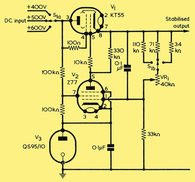
A practical series stabilising circuit.
The design is taken from 'Series Voltage Stabilisers', Application Report No. 1, published by MO Valve Co. Ltd.
A practical circuit for obtaining a stabilised supply in the range 200-500 Volts at 0-100 mA is shown. The circuit, by M-OV, uses a KT55, Z77 as well as the reference tube. The DC amplifier stage, V2, is biased by the use of a QS95/10 voltage stabiliser tube. (If extremely good stability is required, a QS83/3 voltage reference tube should be employed.) Cathode bias cannot be used in this circuit.
The switch wafers S1a, and S1b are ganged. The switch position must be selected so that the desired output voltage can be obtained. VR1 is the fine output voltage control.
The output of this circuit does not vary by more than about 10 millivolts as the load current varies from 0 to 100 mA. The regulation is about 1 Volt for variations of +21% to -7% of the input voltage.
|