|
Descriptions have appeared1, 2 of storage devices for use in serial operation calculating machines, but in this country at least, little emphasis has been placed on the other possible type of computing system, namely, that employing parallel operation. It is not proposed to give any discussion of computing machines in this paper but for completeness it must be stated that in serial operation machines the digits of a number become available, and are used, one at a time starting usually from the least significant, whereas in a parallel operation machine all the digits of any number become available at the same time.
Without wishing to become controversial, it may be remarked that von Neumann, who was the originator of many of the current ideas on calculating machines, has abandoned the serial operation machine in favour of its parallel operation counterpart.
Requirements of a Storage Device
In either type of calculating machine the requirements of the storage similar, and are as follows:
- The storage should be permanent if desired
- The contents of any position must be erasable at will and capable of replacement by new data
- The volumetric efficiency should be high
- The access and replacement time of stored data should be small.
The delay line storage device of Wilkes and the cathode-ray tube memory of Williams satisfy all of the above requirements except (1) and to a less extent (3). Either of these devices loses all its stored data if a power supply failure occurs. In addition, in the forms described by the authors, neither is directly suitable for a parallel operation machine.
The idea of using the well known principles of magnetic sound recording for the storage of digital data seems to have occurred to a number of designers at about the same time, the system to be described in this paper, however, is thought to be the first in actual operation.
Principles of the Magnetic Memory
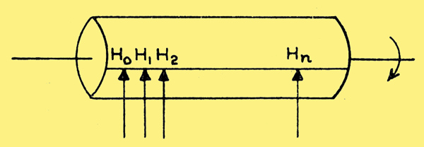
Fig. 1: Magnetic drum and read/record heads.
Essentially, the storage device consists of a cylindrical drum coated with permanent magnetic material and rotating under a. series of read / record heads arranged along a generator of the cylinder. In Fig. 1 H1 - Hn are a set of these heads.
All of the digits of any particular number, which is in binary form (eg, Wilkes), are recorded and read off simultaneously by the heads.
Successive numbers are recorded in sequence as the drum rotates and to distinguish between them an extra track (H0) is added which contains a set of equispaced. positive 'clock' pulses.
In order to determine; the position of the first number it is necessary to indicate the start of this clock pulse track. This could be done in various ways; for example, it might start with a single negative pulse, or alternatively a separate track might contain a single pulse to indicate the zero position of the clock pulse track. In fact, it turns out to be much simpler to leave a small gap, clear of any pulses, at the end of the clock pulse track, and to use this as a zero indication. The general appearance of the magnetic state of the clock pulse track is then shown in Fig. 2.
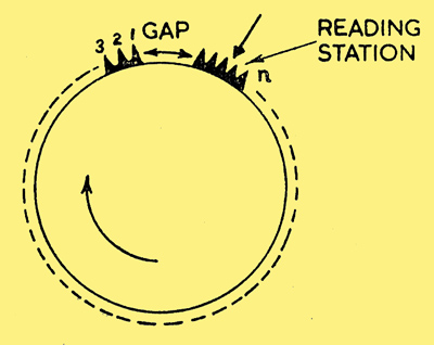
Fig. 2: Magnetic state of clock pulse track.
In order to go to any position on the drum and to read or record there, all that is necessary is to count from the zero position on the clock track and to arrange that the counter emits a. pulse when it reaches the given position. A schematic diagram of the whole memory is given in Fig. 3.
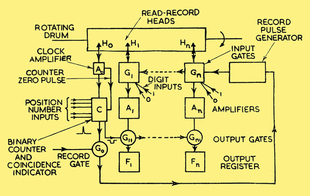
Fig. 3: Schematic of magnetic storage.
The positive pulse input from the clock track head is amplified and sent to the binary counter C, which is arranged to zero on receipt of a pulse from the shaping circuit contained in A0
The contents of C are compared with the required memory location as shown by a set of position number inputs; when the two numbers agree a pulse is emitted by a circuit. Normally this pulse opens a set of gates G11-Gn1, which allow the output pulses from the digit track heads H1-Hn to set a series of flip-flop storage elements F1-Fn to the digit pattern recorded under the heads in the given position. When it is desired to record in a given position a gate G0 allows the above coincidence pulse to trigger a 'record pulse' generator which sends either positive ('1') or negative ('0') pulses, via the input gates G1-Gn, to the heads. It should be noted that prior to the record operation the input gate will have been set to '0' or '1' positions from digit input leads, and that the nature of the storage is such that the input data automatically erases that already present.
In the present memory, intended for use with ARC, (Automatic Relay Computer), the input. gates G1-Gn, the record gate G0 and part of the counter-coincidence circuit are relay elements, and the output flip-flops set relays to operate the remainder of the machine
The Magnetic Circuit
While many highly specialised magnetic recording media exist, these are at present difficult to obtain in suitable form, and it was decided to use a thin plating of electrolytic nickel. Although the magnetic properties of this seem to leave much to be desired, the medium is quite good enough for the purpose in hand. In the final design at plated layer between 0.0005 in, and 0.001 in. in thickness was used. Extensive experiments showed that up to 100 digits/in. could be recorded, but for safety it was decided to use only a 50 digits/in. packing as this allowed for considerable variations in head construction. The surface speed of the drum was 25 ft./sec.
The first models of the recording heads were of the form shown in Fig. 4.
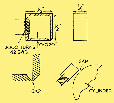
Fig. 4: Early recording head.
Single laminations of 0.020 in. silicon iron were used and the heads were run in contact with the cylinder as shown. Using 2,000 turns on the magnetising coils it was found that the shortest recording pulse which could be used was 35 μsec. This left much to be desired and further experiments were instituted.
About this time Dr Julian Bigelow suggested using a single, very fine wire as recording head.
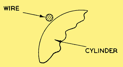
Fig. 5: Single wire head.
This was to be mounted in close proximity to the drum surface and pulsed with a current of between 10 and 50 Amps. Since the current flows for considerably less than 1 μsec. this does not damage the wire. It can be shown that if the input pulse is short enough for the recording medium not to move appreciably during the pulse, the output voltage follows the law:
Eout = K v2it / (4a2 + v2t2)
where
v = surface speed of medium
i = recording current
a = distance of wire centre from drum surface
t = time.
The general form of this function is shown in Fig. 6.
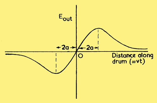
Fig. 6: Output voltage from single wire head,
In the present memory, with digit packing of 50 in., it follows that for non-interference of pulses 4a « 0.020 in. or a « 0.005 in.; this means that wires of diameter less than 0.002 in. must be used. Handling becomes difficult with 0.001 in. diameter wire and problems arise in the design of step-up transformers for ratio of 1:100 and bandwidths of 250 kHz. where the input impedance is about 1 Ω
As a comparison, tests were made using a 0.002 in. diameter single wire and a single lamination head of the general type shown in Fig. 4, but reduced to one-half the linear dimensions. With ten turns. this gave precisely the same output as the single wire, thus indicating losses of about 90 per cent.
It had been evident that the performance improved as the linear dimensions of the heads decreased and a series of experiments were tried with very small heads. These resulted in the design shown in Fig. 7.
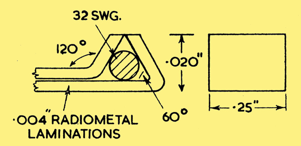
Fig. 7: Final head design.
Using a single 32-gauge wire as magnetising source, the output signal was three times greater than that from a 0.001 in. diameter wire, indicating that the loss in efficiency is no longer important. With the same design it proved possible to insert four turns of 42-gauge wire through the window and 12 times the single wire head output was obtained. The output pulse shape is identical with that of Fig. 6.
In order to record '1' and '0' on the medium the simple procedure of pulsing the head with sufficient current to cause magnetic saturation of the nickel was adopted. Thus, if '1' is recorded with a pulse of +20 Amps, to record '0' a -20 Amp pulse is super-imposed.
Mechanical Construction
A photograph of the cylinder and head assembly is given in Fig. 8.
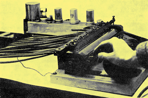
Fig. 8: Model of drum with heads mounted in position.
For mathematical reasons it was decided to have 21 binary digit numbers and to store 256 such quantities. With the packing of 50 digits/in and surface speed of 25 ft/sec., this resulted in a cylinder 2 in in diameter and 12 in. long rotating at 3,000 rpm. The maximum waiting time for reading or recording is 20 m.sec. and the mean time 10 m.sec.
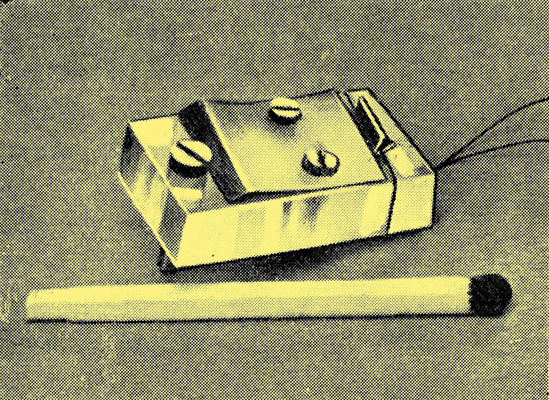
Fig. 9: One of the final read/record heads.
The heads, shown in detail in Fig. 9, are mounted on a brass bar and are individually adjustable by means of a simple screw assembly. Coarse adjustment is provided for aligning the main bar and the drum surface.
Circuits
At the outset it can be stated that all relays are of the Siemens high speed variety with 1000 + 1000 Ω coils. The measured time of closure or operation of these is less than 2 m.sec. Relays are drawn in the normal position.
The Clock Track Amplifier
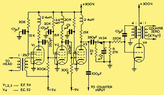
Fig. 10: Clock pulse amplifier, shaper and counter zero generator. EF54 & EC52.
On this track it is necessary to reproduce with accuracy the sharp transition between the two turning points in output voltage shown in Fig. 6, and it was decided that a bandwidth of at least 200 kHz, was needed. The amplifier circuit of Fig. 10 proved adequate.
It will be noticed that the grid coupling and screen resistor by-pass time constants are so chosen that there is a steep reduction in gain below 10 kHz. This makes the amplifier very much more stable and makes inter-stage decoupling unnecessary. In particular, 50 Hz pick-up and microphonic noise from V1 are imperceptible. V3 is biased below cut-off to enable the noise background from the medium to be clipped off. This is necessary, since the gap at the end of the clock pulse track (Fig. 2) may contain a noise pulse of sufficient amplitude to trigger the counter after it has been set to zero.
The output of V3 is fed directly to the input of the binary counter and a portion is rectified by the 1N34 germanium diode and applied as a negative potential to the grid leak of the blocking oscillator tube V4. This keeps the latter from firing until the clock pulse track gap is reached, when the charge on C leaks away via R. The firing of V4 sends a pulse via the output winding of T to the grid load resistor of the counter, thus 'zeroing' the latter.
The Counter and Coincidence Sensor
The counter used is an ordinary scale-of-two circuit with buffer amplifier to remove unwanted pulses. The circuit constants are chosen so that the counter is reliable up to 100 kHz.
Counter Unit
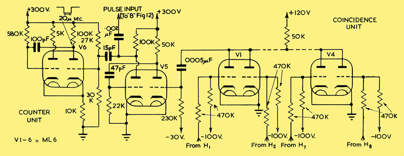
Fig. 11: Counter and coincidence unit. ML6.
V6 generates at negative pulse of 220 Volts amplitude and 15 μsec. duration which is used to gate the outputs from the digit amplifiers into their respective flip-flops.
The Input Pulse Generator
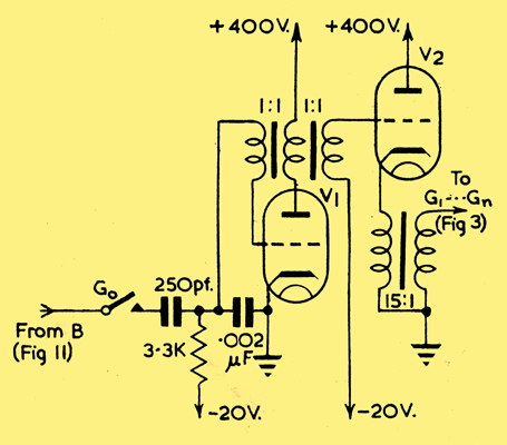
Fig. 12: Input pulse generator.
Since the heads have an input impedance of less than 0.1 Ω and require pulse currents of 10-20 Amps, a special generator had to be designed. Thyratron circuits were tried, but were found to be unreliable and liable to parasitic oscillation. Eventually the circuit shown in Fig. 12 was devised and gives completely satisfactory results.
In the present memory the record gate G0 is a relay, but it would be simple to substitute an electronic element. In the absence of a gating pulse via G0 the blocking oscillator is held off by the bias. The transformer produces a pulse of less than 1 μsec. duration and the cathode follower transformer enables the whole head array to be pulsed.
The Input Gates
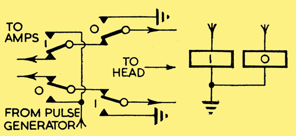
Fig. 13: Relay input gate.
These are constructed from relay elements. and are shown in Fig. 13. Each gate element consists of two relays having two change-over contacts which are activated from the main circuits of the machine. When relay '1' is operated the head is pulsed in the positive sense, and when relay '0' is operated in the negative sense.
The gate action isolates the digit track amplifiers during pulsing, as the stray pulse which crosses the relay contacts due to capacitative coupling does not effect the input transformers, which have extremely low input impedance.
The Digit Amplifiers
These are perfectly straightforward R-C coupled amplifiers, again constructed to give low gain below 10 kHz. A typical circuit is shown in Fig. 14.
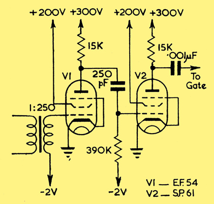
Fig. 14: Typical digit amplifier. EF54 & SP61.
The Output Gate
It is desired to gate the amplifier output into a flip-flop circuit at a given position. only, the two possible amplifier output pulse shapes being shown in Fig. 15.
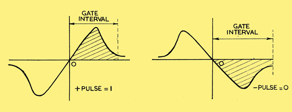
Fig. 15: Output waveforms for '1' and '0'.
Since the clock pulse occurs at the origin in the above sketches, it is possible to generate a gate signal which extends over one-half of the output pulse only, and thus: to select a positive or negative pulse corresponding to unity or zero. Most of the published gate circuits have the disadvantage of placing the output on a 'pedestal' as shown in Fig. 16, or else of transmitting pulses of one sign only.
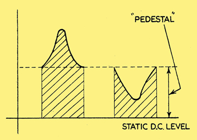
Fig. 16: Output from common gate circuits.
To remedy this defect the circuit of Fig. 17 was devised.
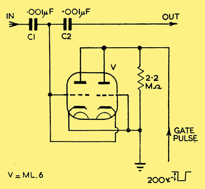
Fig. 17: Gate circuit. ML6.
In, the absence of a gate pulse the twin triode grids act as diodes and short-circuit incoming signals on either sign to earth. On applying a large negative pulse to the two anodes the electrons are repelled to the cathodes and the resistance of the grid circuits rises sharply. If, in this condition, a voltage variation occurs on C1 it is transmitted via C2 to the flip-flop; in the absence of the gate pulse, however, nothing passes.
The Output Stage
This consists of the standard cathode-coupled toggle, shown in Fig. 18.
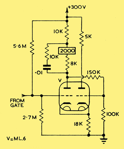
Fig. 18: Toggle output circuit. ML6.
For reliable operation it was necessary to compensate the inductance of the relay coil, and the network shown behaves like a pure resistance.
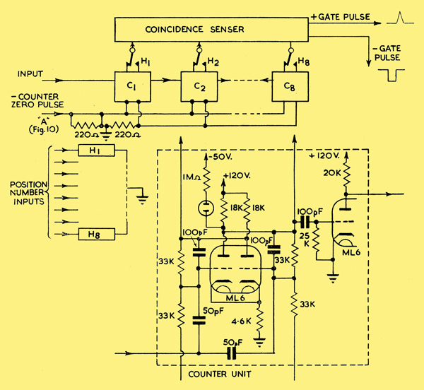
Fig. 19: Counter and coincidence sensor. ML6.
Conclusion
It will be seen from the above circuit descriptions and from the photograph of Fig, 8 that the storage system described in this paper is considerably more compact than any hitherto disclosed. Although in its present form it is somewhat slow in operation it is quite easy to speed up the rotation of the cylinder and to record and read data at several stations around the drum. In this way availability times of better than 1 millisecond could be realised. Work is at present proceeding along these lines and it appears that the necessary modifications are trivial in nature.
The author wishes to express his sincere thanks to Dr Geoffrey Gee, Director of Research, and to the Board of the British Rubber Producers Research Association for supporting this work, and also to Miss X Sweeting and Dr R W Williams for assistance in construction.
References
- Wilkes and Renwick Electronic Engineering 20. 208, (1948)
- Williams and Kilburn, Journal IEE (In press).
The biography referenced in the title block is also here as a pdf.
|