|
Researchers at GEC are leading the way in the creation of whole families of new microelectronic devices based on a technology that electronics had almost forgotten.
Until the 1950s, all active electronic functions were performed by the vacuum valve. In general, these were made up of metal electrodes suspended in a vacuum sealed glass envelope. Their sizes varied, but even the Nuvistor, one of the latest valves to be brought out in a metal ceramic envelope, had a volume of more than one cubic centimetre. It was not surprising therefore that when solid state devices were invented, one of their main attractions was their small size. As the technology developed, individual elements became smaller and smaller, until complete circuits could be designed on a single piece of silicon. This exciting development resulted in the gradual displacement of vacuum valves in receivers and low-power electronic systems. In high power transmitters vacuum valves continue to survive; and thermionic emitters are still used where a free source of electronics is required as in cathode-ray tubes. In addition, the high impedance of valves led to the production of high quality hi-fi and radio systems, and indeed many audio enthusiasts still insist on their superior performance.
Semiconductor devices are poorly equipped to survive certain environments and there is a need for devices which can work at high temperatures, withstand high voltage pulses and have the potential to provide high frequency operation. Vacuum valves offer such properties. Ironically, it is the semiconductor fabrication technology which has been developed over the past few years which now offers the opportunity of producing vacuum valves as small as transistors.
Electron Emission
The operation of any vacuum valve depends on obtaining electrons from the cathode surface and attracting them to a positively-biased electrode known as the anode. The old type of valve operated with a thermionic cathode which was heated to give the electrons sufficient energy to surmount the surface barrier, escape into the vacuum and be attracted to the anode by a positive potential. The cathode was coated with an oxide layer to reduce the work-function and thus the energy required for an electron to escape (and it was heated to over 1,000°C).
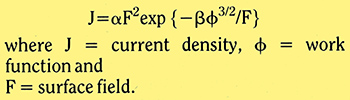
An alternative means of obtaining an electron discharge in vacuum is with field emission. This relies on a very high electric field being applied to a cold cathode which has the effect of thinning the surface barrier and making it triangular in shape. Electrons then have a finite probability of tunnelling through the barrier and being attracted to the anode (Fig. 1).
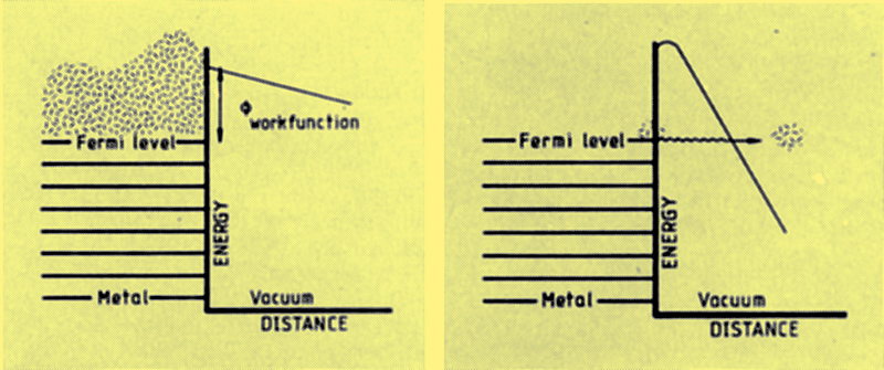
Fig.1a (left): thermionic emission. At high temperatures electrons are excited above the Fermi level and some gain sufficient energy to surmount the surface barrier and escape into the vacuum. Emission is increased by increasing the temperature or decreasing the work function.
Fig.1b (right): field emission. At high electric fields the surface barrier is distorted to a triangular shape. This allows electrons to tunnel through the barrier. Emission is increased by increasing the electric field or decreasing the work function.
Field emission is quite well characterized by the Fowler-Nordheim relation:
Current density increases with increasing electric field and a reduction in work function. Electric fields of the order 109V/m are necessary before an observable current may be obtained; this is equivalent to 1000 V across 1 μm (1 ×10⁶m). Since most solid dielectrics can withstand little more than 108V/m, clever lithographic techniques are used to construct devices which enhance the electric field around the emitting area only.
Applications
There are many potential applications of vacuum microelectronics, but they all centre on the properties of field emitting devices. For example, raising the temperature of such a device will result in simply increasing its efficiency - for in addition to tunnelling electrons, the process will be combined with a proportion of thermionically-excited electrons escaping from the cathode surface. Technology can therefore be directed towards producing sensors and controllers in environments which are subjected to quite harsh temperature fluctuations such as those in boreholes, oil wells, nuclear reactors and jet engines.
For many years a great deal of effort has been directed towards finding a cold electron source to replace the thermionic cathode in such devices as cathode ray tubes, travelling wave tubes and microwave power amplifiers since this would be beneficial in terms of operating power and heat dissipation. Most of these efforts have been disappointing, through short lifetimes and erratic emission. Only recently has our fabrication technology allowed dimensionally accurate reproduction of sub-micron structures, and it has brought totally new opportunities in the control of cold emission.
There has been a growing concern over the malfunctioning of electronic components in space and defence systems when exposed to both ionizing and electromagnetic radiation. Semiconductor devices rely on the excitation of minority carriers for their operation. When exposed to ionizing radiation, they are bombarded by both neutral and charged particles, which cause fluctuations in current leading to failure of the device. The result may be transient upset or permanent damage. Vacuum valves are far more immune to such environments since the source of electrons is that of either a metal or highly-doped silicon cathode.
Vacuum valves work at much higher voltages than semiconductors which makes them far less sensitive to the large voltage pulses experienced, for example, during a lightning strike. The limitation is the current carrying capability of the electrodes themselves. In addition, the speed of a semiconductor device is basically limited by the time taken for an electron to travel from the source to the drain which in itself is limited by the number of collisions within the lattice of the solid. Vacuum valves, however, operate by electrons passing from cathode to anode within a vacuum and their passage is therefore unimpaired by molecular collisions. With dimensions of 1μm transit time of less than 1ps can be expected.
In any protection device which operates by short-circuiting the delicate components, it is necessary that the initiation takes place before the transient pulse causes the damage. Current surge arrestors exploit a discharge in an ionized gas which for certain applications does not operate rapidly enough. The combined properties of speed and survivability in hostile environments lead to the applications of very fast protection devices in communication systems, high-integrity logic elements and radiation-hard integrated circuits.
Since this same technology can also be applied to the realization of large area, full-colour, high brightness flat panel displays, a separate section of this article will be dedicated to this subject.
Electron Sources
Most research programs in this field are concentrating on cold cathodes to take advantage of the small device size, instant start, low power consumption and high current densities which in turn will lead to high operating frequencies and fast switching.
Until last year, however, there was a major research programme at Los Alamos which produced miniature thermionic electronic components. This technique used thin-film deposition and photolithographic techniques to produce integrated structures consisting of a grid and an oxide-coated cathode on one substrate, with an anode on a separate substrate directly opposite.
A different approach has been reported by the Philips Research Centre in Eindhoven which has exploited the strong internal electric field in a semiconductor with a reverse-biased p-n junction. A preliminary investigation was undertaken on various cathode geometries, but efforts were finally concentrated on a design which produced high current densities when the 1μm diameter emitter was about 10nm below the surface and parallel to it. In 1987 these cathodes were producing 1500A/cm2 with 1.5% efficiency. [1] G G P van Gorkom, A M E Hoeberechts, Philips Technical Review, Vol. 43, No 3, January 1987
When a p-n junction is reverse-biased a very strong field is created in the depletion region. Electrons coming from the highly doped p-region are therefore accelerated and gain energy. Although much of this energy is lost in collisions with other electrons or optical phonons, a percentage of electrons have sufficient energy to surmount the potential barrier at the surface and escape into the vacuum. To improve the efficiency of the device, the work function is reduced by covering the surface with a monolayer of caesium. The complete structure consists of the p-n junction, as described, with an overlying gate above it separated by silicon dioxide. Such structures have already been incorporated into small cathode ray tubes to give clear, bright and well defined black and white and colour pictures.
The major area of interest in other groups is in lithographically defined sharp-tipped structures, which are incorporated into a diode configuration, and make use of a grid about 1μm away to create a very high field around the tip, which will then emit electrons. The typical structure is shown in Fig. 2, and is made up of small cathodes 1-2μm in height, with sub-micron (∼50nm) emitting tips. These are separated from a metal grid 0.5μm thick by a layer of silicon dioxide.
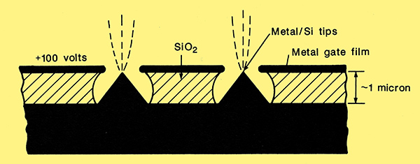
Fig.2. A typical field-emitting device consists of a metal or silicon substrate, with a number of small sharp tipped structures about 1-2μm high and 10mu;m apart. These have tip radii of about 50nm and are separated from an integral grid by 1-2μm of silicon dioxide. The structure is operated by applying a positive voltage of 100-200 V to the metal grid, which creates a high electric field around each of the emitting tips from which electrons are emitted. These can be collected either on the grid itself of by an external anode held in close promixity to the tips. At SRI International, Menlo Park, structures such as these have given currents of 100μA/tip leading to current densities of 100 A/cm2 and lifetimes of over 60, 000 hours.
A number of techniques may be used to produce such structures and these include the anisotropic etching of silicon, etching of a unidirectionally solidified eutectic system and the use of deposition techniques and UV or electron beam lithography.
The well-established team at SRI International in Menlo Park, California, USA, has published details of both fabrication procedures and the electrical characterization of field emission structures. To construct the diodes, they deposit on a substrate material first silicon dioxide and then molybdenum. Electron beam lithography is used to define the grid holes and the silicon dioxide removed down to the substrate. The next process is to evaporate aluminium at an angle whilst rotating the sample, which has the effect of reducing the diameter of the grid hole. This is followed by molybdenum deposition perpendicular to the substrate, and a lift-off procedure to remove the aluminium and excess molybdenum [2] C A Spindt, C E Holland and R D Stowell, J Phys., 9,269-278, 1984.. This produces very fine-tipped conical cathodes between each grid hole. At gate voltages in the region of 120 V, current densities of over 100A/cm2 have been obtained and lifetimes of over 60 000 hours.
Developments at GEC
GEC Hirst Research Centre is undertaking a research programme to investigate electron emission from novel structures with the long-term aim of producing a new range of micron-sized vacuum electronic devices. The programme began as a small feasibility study in July 1986 and has grown rapidly over the past two years because of the encouraging results obtained and the increasing need for such devices. GECs is now the largest team in Britain.
The programme consists of two projects running in parallel. The first concentrates on using lithographic definition of electrodes to create the high fields necessary for field emission, while the other is a longer-term programme to examine the fundamentals of electron emission in greater depth, with particular reference to noise, stability and reproducibility. In addition, methods are being explored whereby electrons are emitted from planar, chemically-modified surfaces, at electric fields some two orders of magnitude less than those conventionally associated with field emission. Preliminary results [3] N A Cade, G H Cross, R A Lee, S Bajic, R V Latham, J Phys. D, App. Phys., 21, 148-153, 1988. have already shown that a cathode covered with a thin layer of organic film will produce emission sites at 102V/m. Research is being undertaken to clarify the mechanisms involved in such a process.
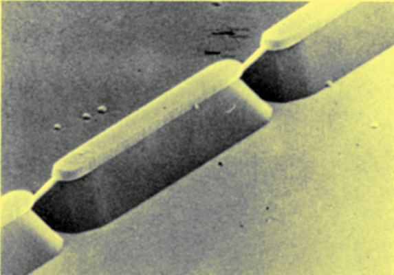
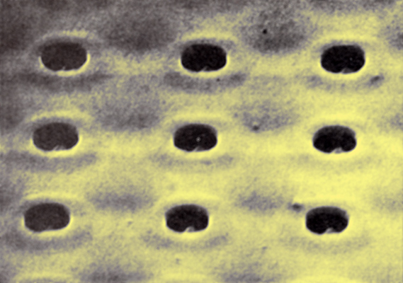
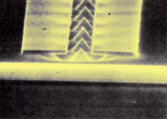
Significant progress has been made within Hirst Research Centre in developing a method of fabricating field emitting diodes suitable for a manufacturing process. A variety of wet and dry etch techniques have been perfected to form micron-sized cathodes in both metals and semiconductors(Fig. 3).
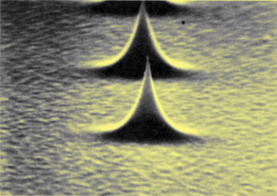
Fig.3. Silicon, niobium and gold emitters.These and the other photographs were produced at the GEC Hirst Research Centre.
A partially etched wedge-shaped emitter 10μm long.
2μm high silicon emitter with 30nm tip radius.
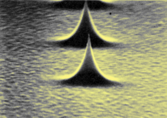
Array of gold emitters 2μm high.
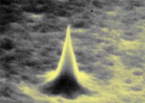
Niobium emitter 1.7μm high.
The latter have been incorporated into a triode configuration consisting of an interdigitated anode/grid structure, using the 2μm-high miniature cathodes with submicron emitting tips and attaining packing densities of up to 2.5 × 10⁷ tips/cm2. The procedure exploits standard semiconductor fabrication technology on four-inch silicon wafers; and one method by which the silicon structures are produced is depicted in Fig.4.
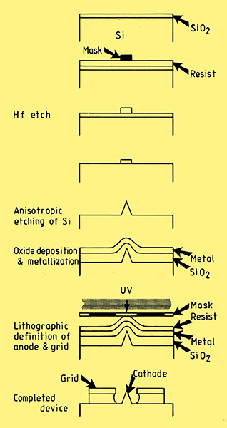
Fig.4: Processing sequence for the fabrication of silicon field emitting diodes.
A thin layer of silicon dioxide is thermally grown on a wafer of single crystal silicon, and patterned using standard UV lithography and etching techniques to form small pads of SiO2 (1-2 μm square). A wet anisotropic etch then attacks the different planes of silicon at different rates which results in the formation of pyramidal shaped structures which may be sharpened in a number of different ways. Dielectric deposition and planarization is then followed by metallization and the definition of gate electrodes. The final process step is the cavitating etch to remove dielectric from around the emitting tips. Each 2 mm chip is mounted in a 16 pin dual-in-line ceramic package using a gold/silver eutectic and tested within a vacuum system capable of attaining 10-9 torr.
Preliminary results are very encouraging, with true diode characteristics observed (Fig. 5) and currents of up to 10μA obtained at 200-300 V grid voltages from 80 n-type silicon emitters. Work is progressing rapidly towards the incorporation of metal emitters with the hope of attaining still higher current densities. Results from the SRI International programme show a realistic longterm aim of 10μA/tip or 100A/cm2 at operating voltages of 100-200V.
Considerable electrode damage may be caused by a switch-on process during the initiation of electron emission but this can be much reduced by surface cleanliness. To study the effects of surface contamination, an ultra-high vacuum system with surface science facilities is being used (Fig. 6).
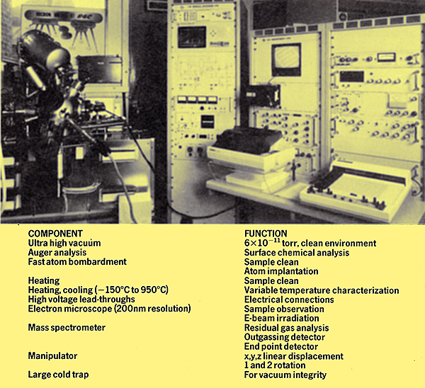
Fig.6. Ultra-high vacuum system for surface and electrical characterization.
It is important to clean the cathode surface thoroughly before making electrical measurements and this is achieved using fast atom bombardment and sample heating. Since monolayers of contaminants will form quite rapidly over the cathode surface the residual gases are analysed by a mass spectrometer and the chemical integrity of the surface is monitored by Auger analysis. An electron microscope with 200nm resolution is used to observe the device during and after operation, for detecting defects; this accelerates design optimization. The system itself can be evacuated to 10-11 torr and filled with a variety of gases so that operation under different environments may be examined. It has already been demonstrated that stable emission may be obtained at atmospheric pressure in inert gases.
It is important to remember that these devices have electrode separation of about 1μm, which is much smaller than the electron mean free path at 10-5 torr. This is of utmost importance when final packaging of devices is undertaken, since evacuation to 10-11 torr would be impossible in packaged isolated devices.
Flat Panel Displays
Cathode-ray tube technology is 86 years old. It allows inexpensive black and white and colour display screens of varying sizes; but for many years there has been a demand for less bulky and portable flat panel displays having lower power consumption, improved contrast, brightness and full-colour definition. The three main contenders for replacing the CRT are the liquid crystal, gas plasma and electroluminescent displays. The liquid crystal displays (LCD) rely on the properties of aligned molecules which turn in an electric field. In the simplest form the liquid is held in a thin cell between two polarizers. In the off state, light is reflected, but in the on state an applied voltage realignment allows light to be absorbed by one of the polarizers. The LCD fulfils the requirements for size, weight and low operating power, and 14-inch diagonal displays have been successfully made with 960 x 1284 pixels. The main problems associated with LCDs are those of poor yield and high manufacturing costs when large screens are considered. Nevertheless they have already captured over half the total market for flat panel displays.
Gas plasma displays (CPD) rely on gas excitation between two electrodes which cause light to be emitted. Although there is no need for back-lighting, the required power is still greater than that of LCDs. Substantial progress has been made, however, and while existing displays are confined to 16 levels of grey, there is a promise of 15-inch full-colour screens having 256 000 pixels. However, previous attempts to make full colour displays have had mixed success.
Electroluminescent displays (EL) use phosphors which emit light in the presence of an AC field. These give better contrast and broader viewing angles than other flat panel displays, and require less power than both CRTs and CPDs. These lightweight, compact displays are stated to be more reliable than CRTs with predicted lifetimes of 40 000 hours, though this has not yet been confirmed. In addition they are reliable in hostile environments, and are therefore important in military applications.
At present EL displays are quite expensive, four times the cost of an equivalent-size CRT display, but this is expected to drop to 50% by 1990. Displays of 12 x 14 inches have been made, with 640 x 400 pixels. The low level of brightness and the lack of a full-colour screen are the main disadvantages; and while good colours have been achieved with both red and green phosphors, it is difficult to produce bright blue emission. Both EL and GPD have the disadvantage of a lack of full colour. Furthermore they use expensive high-voltage devices.
Field-emission Flat Panels
Field-emission flat panel displays have the advantages of high brightness, good contrast, low power consumption and full colour. In addition they are expected to be reliable in hostile environments. With each tip giving 10μA, a 10 x 10 array provides sufficient current for one pixel. The large number of emitters in one pixel tends towards a uniformity in emission and the fabrication is suitable for large areas of individually-addressable pixels. Cathodes have been shown to operate well in vacuums of 10-5 torr and since the average electron mean free path is greater than the electrode separations, the life expectancy is long since the cathodes will not be plagued by erosion from ion back-bombardment. The team at SRI has already produced a full-colour display using this technology on a five-inch silicon wafer baseplate [4] C E Holland, C A Spindt, I Brodie, J B Mooney and E R Westerberg. Presented at Eurodisplay 1987. with three colour elements and 114 244 individually-addressed pixels.
Part of a 10 x 8 array of emitters at 10μm pitch with an Al/Si integral grid.
Pyramids at 2μm pitch in a grid channel.
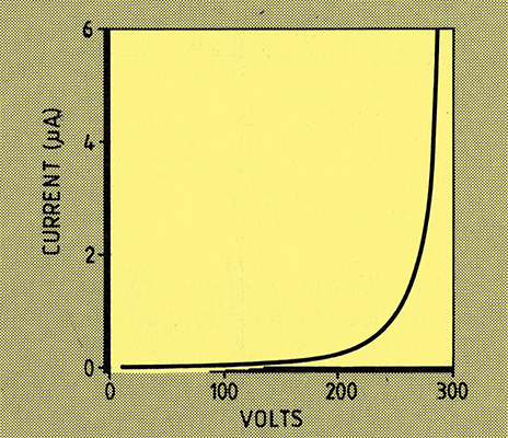
Fig.5: n-type silicon emitter incorporated into a diode configuration (above), and its corresponding electrical characteristics.
The screen is coated with indium tin oxide and patterned with strips of colour phosphor, each 60μm wide. The cathodes with integral grid are separated from the screen by small pillars about 75um high which allows a voltage of up to 1000 V to be applied. Each 250μm pixel is addressed by contacting the cathodes from a molybdenum backplate 175μm wide in one direction, and the three 40μm gate electrodes orthogonal to this. The matrix is operated by sequentially addressing one line at a time in the horizontal direction while simultaneously driving all the gate lines in the vertical direction. Very high brightness has been achieved with green phosphors at 200 V, but so far the red and blue phosphors require 500 V. Dimensions are therefore quite critical in terms of voltage for optimum brightness without precipitating the onset of vacuum breakdown. The whole plate is vacuum sealed after baking at 125°C for 12 hours which achieves a pressure of 10-10 torr. If emissive flat panels are to take a significant fraction of the market this relatively late starter looks very promising, and while many major assembly and processing problems have been overcome, there are many technical issues to be addressed before a useful display is placed in production.
The Future
Reproducibility, stability and noise level are amongst the problems associated with field emitting devices. Solutions must be found before we shout 'eureka' and sail forward into production. Expectations are high, however, as we look forward to the understanding and control of electron emission emerging from our research programmes.
The First International Conference on Vacuum Microelectronics was held in Williamsburg last year, with over 200 attending from France, Holland, Japan, Russia, USA and UK. Britain is hosting the Second Conference in Bath in July and is already attracting much interest from both academic and industrial organisations world-wide.
References
- G G P van Gorkom, A M E Hoeberechts, Philips Technical Review, Vol. 43, No 3, January 1987.
- C A Spindt, C E Holland and R D Stowell, J Phys., 9,269-278, 1984.
- N A Cade, G H Cross, R A Lee, S Bajic, R V Latham, J Phys. D, App. Phys., 21, 148-153, 1988.
- C E Holland, C A Spindt, I Brodie, J B Mooney and E R Westerberg. Presented at Eurodisplay 1987.
* Dr Rosemary A Lee - GEC Hirst Research Centre, Wembley, Middlesex.
|