|
In spite of the fact that resistance coupling is one of the oldest forms of inter-valve couplings, it is still widely used and offers great advantages over other types where the highest standard of quality of reproduction is desired. Moreover, it finds wide application for television purposes. If distortionless amplification is to be secured with resistance-capacity coupling, it is necessary to pay at least as much attention to the voltages which are applied to the valve as to the values of components. Great care is necessary in selecting the operating conditions of the penultimate valve. The design of such an amplifier is more complex than is often realised, and is dealt with in detail in this article.
Although resistance - capacity coupling is often thought to be the remedy for all distortion difficulties in low-frequency amplifiers; it is not so unless the correct values are assigned to the various components. Empirical rules exist for selecting values, but they are useful only. in certain cases, and are not of universal application.
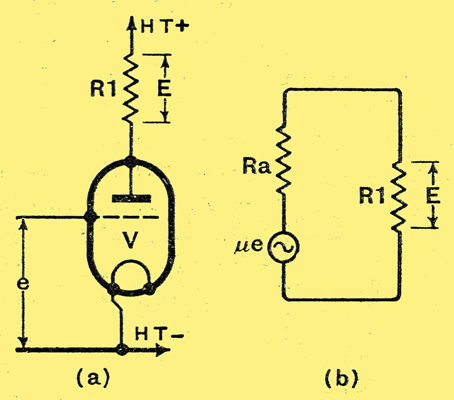
Fig. 1. - The fundamental circuit of resistance coupling is shown at (a) and the equivalent circuit at (b), in which μe and Ra are a generator and resistance which replace the valve.
In designing an amplifier there are two main types of distortion to consider frequency and amplitude distortion - and the former is much the easier to treat. Let us, therefore, consider it first, The principle of resistance-coupled amplification is simple, and is illustrated in Fig. 1 (a). We have a valve with an amplification factor μ and an internal resistance Ra, and we apply an input voltage e to the grid circuit. A resistance R1 is included in the anode circuit and the voltage E developed across this is the voltage applied, to the next stage. It is easy to see that the amplification A = E/e.
When considering the action of a valve the simplest course is to represent it by a resistance equal to its internal AC resistance in series with a perfect generator supplying a voltage μe, as shown in Fig. 1 (b). It can now be seen at a glance that the fraction of the voltage μe which appears across R1 depends upon the relative values of the two resistances expressed mathematically, A = μR1/(Ra + R1). It can be seen, that A = μ when R1 is infinitely great, and that A can never exceed this value; the amplification with resistance coupling is consequently limited by the amplification factor of the valve. When R1 is very small compared with Ra the amplification is only a small fraction of μ and is nearly proportional to R1. When R1 is greater than Ra, however, the amplification begins to approach μ, but is only affected to a small degree by changes in R1. If R1 be made equal to Ra the amplification becomes equal to one half the amplification factor of the valve (μ/2). If R1 = 3Ra then A = 075μ; if R1 = 10Ra, then A = 0.908μ. For a variety of reasons to be discussed later it is unwise to use too high a value of coupling resistance, and R1 is not usually greater than three times Ra, so that the amplification obtained is about three-quarters of the valve amplification factor.
An amplifier of this type contains no reactance and is consequently entirely free from frequency distortion. In practice, however, the simple circuit of Fig. 1 does not hold good, for two factors enter to introduce distortion. The first factor is the stray capacity inevitable in any practical amplifier, and the second is the coupling capacitor necessary for transferring the amplified voltage to the following stage. The question of the grid leak must also be considered.
Stray Capacities
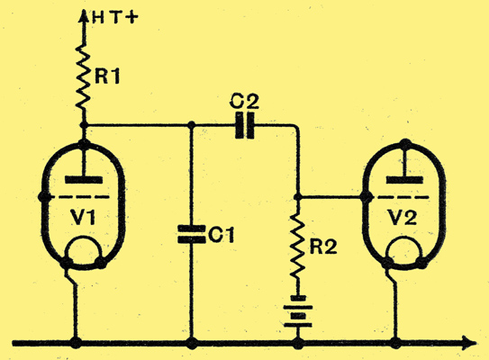
Fig. 2. - In a practicalb amplifier; C2 and R2 are needed to obtain the correct DC grid potential on the following valve, and the inevitable stray capacities provide C1.
A practical stage of amplification, therefore, takes the form shown in Fig. 2, in which the valve and R1 correspond to Fig. 1. The capacitor C2 is necessary to pass the variations in potential which appear across R1 to the grid of the following valve, while isolating it as far as direct current is concerned. The grid leak R2 is needed in order to permit negative grid bias to be applied to V2. The capacitor C1 is rarely found as such in an amplifier, and it is usually present as a component only when V1 acts as a detector; it is, however, an inherent part of an amplifier and consists of the anode-cathode capacity of V1, the effective grid-cathode capacity of V2, and the stray capacities of the components and wiring. It is difficult to assess the value of this unavoidable capacity, for it depends to a large degree upon the following circuits: in a case where V1, is an MHL4 valve and V2 is a PX4, the value of C1 is of the order of 150 pF.
At low and medium frequencies the reactance of this capacity is usually at so high in comparison with the circuit resistances that it can be ignored. At high frequencies, however, the reactance falls, and since this reduces the load impedance on the valve the amplification decreases. The presence of this capacity, therefore, sets an upper limit to the range of frequencies over which any given amplifier is useful.
Now let us consider what happens in the coupling circuit. It can be seen that C2 and R2 really form a voltage divider across R1, so that the fraction of the voltage. across R1 which appears across R2 and is applied to the following valve depends upon the relative values of the reactance of C2 and the resistance of R2. It can be shown that at the frequency at which the reactance of C2 equals the resistance of R2, the voltage developed across R2 is 70.7% of that across R1. The reactance of C2 falls with increasing frequency, so that it is only necessary to consider this component at the lowest frequency needed, for the value chosen to satisfy the requirements at this frequency will be entirely satisfactory at any higher frequency.
It will be apparent that we can divide the operation of a resistance-coupled amplifier into three categories according to the frequencies concerned, At a medium frequency around 400 Hz the various capacities exert a negligible effect, and the amplification obtained depends only on the valve and resistances. At the lowest frequency required it is only necessary to employ a large enough capacity for C2 relative to the value of the grid leak R2 for the loss in the coupling to be negligible.. At the highest frequency required C2 can be ignored, and we have so to proportion the values of C1 and the various resistances that negligible loss in amplification occurs.
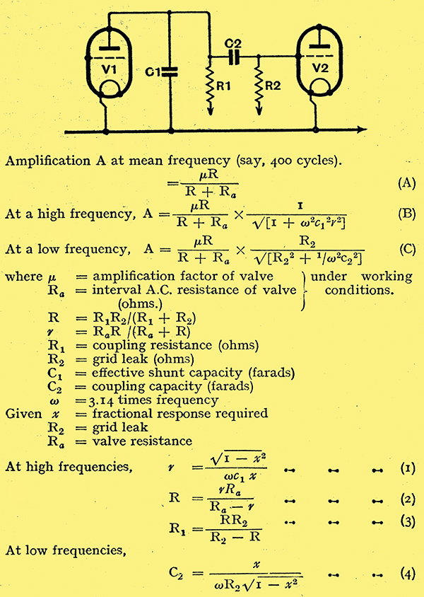
NB. The meaning of the symbol ω was given as 3.14 times frequency instead of 6.28 times frequency.
The various formulae governing the design of an amplifier of this type are given in the table above, and their use will be best understood by an example. Suppose we wish to design a stage of exceptionally good frequency response, and we intend to use a valve of 30,000 Ω resistance for V1. The grid leak R2 cannot usually exceed 0.25 MΩ if V2 is an output valve, for the valve makers often specify this figure as the maximum permissible grid to cathode resistance. If we say that the amplification at the two extremes of 20 Hz and 10 kHz can fall to 95% of that at about 400 Hz, we can write:-
Ra = 30,000 Ω,
R2 = 250 kΩ,
x = 0.95 at 20 Hz and 10 kHz,
C1 = 150 pF.
We then calculate the value of r, which is the valve resistance in parallel with the coupling resistance and grid leak, from equation (1); we have r = √(1 - 0.952)/0.95 × 6.28 × 104 × 1.5 × 10-10 = 10,900 Ω, The next step is to evaluate R from equation (2) and we have R = 1.09 × 3 × 108 30,000 - 10,900 = 17,100 Ω R1 can now be determined from equation (3) as follows: R1 = 2.5 × 1.71 × 109 / 2.5 × 10⁵ - 1.71 × 104 = 18,350 Ω. The next step is to evaluate C2 at 20 Hz from equation (4), and we have C2 = 0.95/6.28 × 20 × 2.5 × 105 √(1 - 0.952) = 3.1 × 10⁻⁷F = 0.31 μF
We can now write down the values of the, components as:-
R1 = 30 kΩ,
C2 = 0.31 μF
The amplification obtained can be calculated from equation (B) for a medium frequency, and we have A = μ × 17,100/(17,100 + 30,000)17,100/(17,100 + 30,000) = 0.362μ, so that we shall obtain 36.2% of the amplification factor of the valve. A battery valve may have μ = 30, so that the stage gain is 10.85 times; a mains valve, however, might have μ = 80, and then the amplification would be 29 times.
The design of the stage is now complete, and we know that we shall find nothing to complain of as regards its frequency characteristic. The question of amplitude distortion must not be over-looked, however. The load impedance, which in this case can be considered as R (R1 and R2 in parallel), exercises a straightening effect on the valve characteristics, which increases with the value of R. It will be shown later that except when the valve is to handle exceptionally small voltages the load resistance R should not be smaller than twice the valve resistance Ra. We have, however, obtained, a value of 17,100 Ω for R, and Ra is 30 kΩ, so that our load impedance will be nearly one-half of the valve resistance. Although our stage is satisfactory as regards frequency distortion, it may fail entirely when we come to consider amplitude distortion.
A note regarding the remedy may be of interest. The correct procedure in a case of this nature is to choose a lower resistance valve, This will not affect the values of C2 and R2, and will probably alter C1 negligibly. We have, therefore, only to determine R1 for the new conditions. Suppose we choose a 10 kΩ valve, r = 10.9 kΩ as before; when we determine R we find it equal to -121,500 Ω, or a negative resistance. What has actually happened is that we have chosen a valve which is itself of low enough resistance to maintain the upper register to the required degree, and no matter how high we make R1 the high-frequency response will not fall below the limit which we have set. Formulae (2) and (3), therefore, are of no use to us in this case for determining R1, and we can choose it solely on grounds of obtaining maximum amplification or minimum amplitude distortion. In general, the avoidance of distortion is of greater importance than the attainment of maximum amplification, and the considerations necessary for this will be dealt with later.
Decoupling Considerations
Before concluding this section it may be as well to remark on two aspects of the coupling which affect the bass response and which are not shown up in the formula. In the first place the bass response will be, slightly greater than that calculated, from equation (C), due to the increase in load on the valve when the reactance of C2 becomes appreciable. At middle frequencies the load consists of R1 and R2 in parallel, for the reactance of C2 is so small in comparison with the resistance of R2 that it can be ignored. At low frequencies, however, the reactance of C2 increases and may become appreciable. The load is then R1 in parallel With the series combination of R2 and C2 and increases with frequency. This effect increases the amplification assessed by equation (C) by a factor
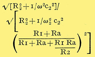
and will be seen to be negligible as long as R1Ra/R2 is small compared with unity.
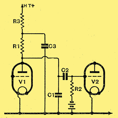
Fig. 3. - When decoupling is included the circuit takes the form shown in this illustration, where R3 and C3 are the decoupling components.
The second effect is one which occurs when decoupling is included; the circuit then takes the form shown in Fig. 3. If the decoupling resistance R3 has a high value compared with the reactance of the capacitor C3, the impedance of the load on the valve will rise at low frequencies owing to the increasing reactance of the capacitor. The effect is similar to that found with the coupling components, but it can occur with greater magnitude. It can be shown mathematically that it can exactly compensate for the loss in the coupling.
In practice this is rarely of great use, for R3 is not often negligible and severely limits the possible rise in load impedance at low frequencies. iThe only case in which the effect maybe put to definite use is where R3 has a high value and R1 a low value (under some 5 kΩ), as in some tone correction circuits, Unless the values be properly chosen it is then easy to obtain excessive amplification of the bass. In general, however, these effects may be ignored and the amplification calculated with sufficient accuracy from the formulae given in this article. The loss of bass experienced in practice is then likely to be slightly less than the calculated value.
The conditions necessary for a minimum of frequency distortion in a resistance-capacity coupled amplifier were dealt with above, and it was shown that the values of components often depend largely upon the internal AC resistance of the valve. Where the valve is of low resistance, however, it was pointed out that there is no optimum value for the coupling resistance from the point of view of frequency distortion, and that a choice should then be made for minimum amplitude distortion. We have, therefore, to settle the best value for this resistance.
Two factors must be known before the conditions can be determined the maximum output required and the maximum harmonic content to be allowed. The maximum output will be equal to the maximum. input required by the next stage, and if this includes a PX4 valve we shall need about 35 Volts peak. The distortion should obviously be kept as small as possible. A total of 5% harmonic distortion is often considered permissible, but if we accept this figure we must not forget that it represents the total distortion of the whole apparatus. If we allow 5% distortion in each stage, we shall find severe distortion when all stages are considered together. It is necessary, therefore, to keep the distortion in individual stages at a minimum, and the writer suggests that it should not exceed 1%.
Dynamic Characteristics
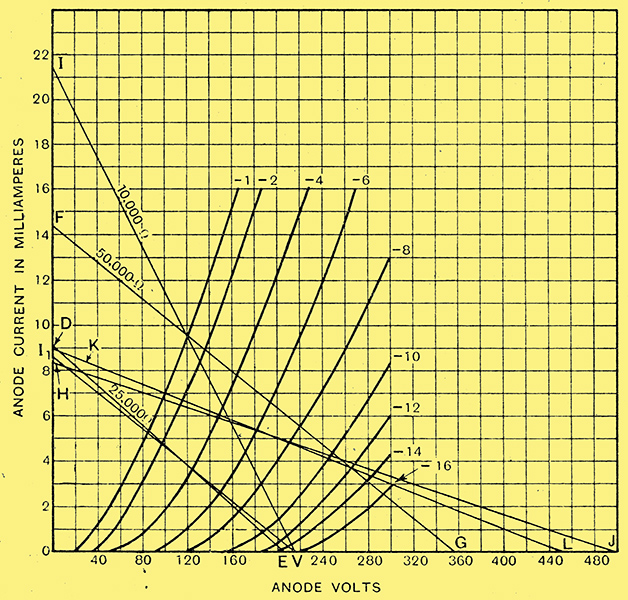
Fig, 4. - The anode-volts anode-current characteristics of an MHL4 valve, together with a number of load lines.
The method of calculation best adapted for the determination of the operating conditions is graphical and is best demonstrated by an example. Suppose we have an MHL4 valve, which has an AC resistance of some 10 kΩ under working conditions and an amplification factor of 20, and we wish to drive a PX4 valve from it with an HT supply of 215 Volts. It was shown before that with such a valve we can use any value of coupling resistance without fear of frequency distortion. We have, therefore, to find the most suitable value of coupling resistance for an output of 35 Volts peak, with not more than 1% distortion. This is most easily done by approximate calculation, after which the results can be checked by a single accurate calculation.
We require a set of anode volts-anode current curves of the valve and these are shown in Fig. 4 for the MHL4 valve. The first step is to mark off the voltage available, in this case 215 Volts, at V; then assume some value of coupling resistance, say 10 kΩ, and mark off a point I on the current scale equal to the current which would flow if the whole volt-age were applied across the resistance. For these conditions, it is 215/10,000 = 0.0215 A. = 21.5 mA join the two points V and I by a straight line, then the intersections of the line with the valve curves enable the actual anode current and anode voltage of the valve to he read off for the case when the coupling resistance is 10 Ω and the HT supply 215 Volts. If the HT voltage is different, then it is only necessary to draw a line parallel with I-V, cutting the voltage scale at the new voltage in order to determine the new conditions.

Fig. 5. - The dynamic characteristics showing the straightening effect of a high resistance load.
Although everything can be determined directly from this diagram, it is usually more convenient to plot the dynamic characteristic of the valve and use this to determine the output, amplification, and distortion. This may be done by plotting the actual anode voltage of the valve against grid voltage, as in Fig. 5. It can be seen that at -1 Volts grid bias the actual anode voltage is 120 Volts, While at -2 Volts it is 131 Volts, and so on.
The amplification obtained can be read off directly from this curve and is equal to the change of anode voltage for a change of 1 Volt in the grid potential; thus at -1 grid Volts the anode voltage is 120 Volts, and at -2 Volts it is 131 Volts, so that the amplification is 131-120 = 111 times. This is slightly greater than the value which would be calculated from the formula in the previous article assuming the valve to be of 10 kΩ resistance, and to have an amplification factor of 20, and the discrepancy is to be accounted for by the fact that under these particular operating conditions the valve resistance is a little lower than 10 kΩ. It must be emphasised that the valve resistance always varies somewhat with the operating conditions.
Now we require an output of 35 Volts from the valve, and we can not operate the valve at a grid potential less negative than some 1 Volt on account of grid current. A peak output of 35 Volts means that the anode potential must vary between 120 volts (the value for -1 Volts grid potential) and 155 Volts (the points A and C on Fig. 5), during the positive half-cycle of input, so that the point C corresponds to the grid bias, and we see that -4.3 Volts is needed. The input is consequently 4.3 - 1 = 3.3 Volts peak and during the negative half-cycle the grid swings to -7.6 Volts and the anode potential becomes 185 volts, corresponding to the point B. We now see that the positive half-cycle of input causes a change of anode potential of 35 Volts, but the negative half-cycle causes a change of only 30 Volts. Amplification, therefore, is not distortionless.
The percentage second harmonic distortion can be calculated from the formula D = 100 ((Emax + Emin)/2 - Enor) / (Emax - Emin) in which Emax and Emin are respectively the maximum and minimum anode voltages and Enor is the anode voltage at normal grid bias In this case we have Emax = 185 Volts, Emin = 120 Volts and Enor = 155 Volts; the distortion, therefore, is 100 ( (185 + 120) / 2 - 155) / 185 - 120 = 5.55%. (This calculation gives 3.85% -Ed.)
Looking at The Valve Wizard site the calculation can be written as (Enor - Emin) - (Emax - Enor) divided by 2 × (Emax - Emin) and then expressed as a percentage. Plugging the figure from the example into this calculation gives D% = (35 - 30)/2 × 65 = 5/130 = 0.3846 × 100 = 3.85% as above. -Ed.
This, obviously, is not good enough for our requirements, so let us repeat the calculation for a load resistance of 25 kΩ. The load line on Fig. 4 now becomes V Ii, and at first glance one would expect more distortion since the line cuts more into the curved portion of the valve characteristics. This is not necessarily the case, however, for the distortion depends-chiefly upon the ratio of the load resistance to the valve resistance. The distortion is due largely to the variations in valve resistance with grid voltage, causing variations in the amplification, and this can be made small by using a sufficiently high value of coupling resistance. We now have a fresh dynamic curve A1, G1, B1 to plot in Fig. 5 for the new load resistance.
The anode potential for -1 Volts grid bias is now 85 Volts, so that the grid bias must be chosen to give 85 + 35 -= 120 Volts steady anode potential, for an output of 35 Volts peak; the grid bias, therefore, must be 3.7 Volts, and the input required is 2.7 Volts peak, so that the amplification has increased: to 12.95 times. The negative half-cycle of input thus reaches 2.7 + 3.7 = 6.4 Volts, and we can read off the values of anode voltage under operating conditions; we find that Emax = 154.5 Volts, Emin = 85 Volts and Enor = 120 Volts. The voltage excursions above and below the mid point are thus 34.5 and 35 with a total excursion of 69.5 Volts. The distortion then becomes 0.5 / 2 × 69.5 = 0.5 / 139 = 0.36%. This is such a satisfactorily small value that we need proceed no further and we can settle on 25 kΩ as a satisfactory value of coupling resistance.
Now this calculation has been only approximate, for we have ignored the effect of the grid leak in parallel to the coupling resistance. The load line to direct current will still be VI1 in Fig. 4, but the line for AC will be different. If the grid leak is 250 kΩ, and the coupling resistance 25 kΩ, the effective load to AC will be 22,700 Ω. Although the DC conditions are still accurately represented by VI1, we must draw a new load line for AC conditions through the intersection of VI1 with the grid bias we intend to use. The amplification with the new load will be slightly less than that previously calculated so that we shall require a little larger input to the valve to maintain the output and an appropriately greater grid bias unless we permit the grid to run slightly more positive than -1 Volt. This is probably permissible in this case, since the change is very small. The new load, therefore, can be drawn for a bias of -3.7 Volts and takes the form DE on Fig. 4. A new dynamic curve can be drawn in Fig. 5, but over the working part of the characteristic the change is exceedingly small, and we can neglect it.
Decoupling
It can be seen, however, that it the coupling resistance and the grid leak are comparable in magnitude the difference between the AC and DC conditions will be great, and the distortion tends to be higher than would be the case with identical DC and AC conditions, and the calculation of the circuit tends to become tedious, It is good practice, therefore, to limit the value of the coupling resistance to about one-tenth of the grid leak resistance, and as the latter is usually limited to 250 kΩ preceding an output valve, we fix on 25 kΩ for the coupling resistance. It will be readily seen that this value is in no way critical; it should not be lower, for this will increase distortion, but it can be made higher without ill effects.
The effect of a decoupling resistance can be allowed for in the same way as a grid leak, for its only effect is to make the DC load higher than that for AC The use of decoupling, therefore, reduces the voltage handling capacity of a valve or increases the distortion. Decoupling is necessary, however, so its effect must be compensated by an increase in the HT voltage. In the example quoted, the HT supply was taken as 215 Volts, and the curves show that under the selected operating conditions the anode current is 3.7 mA. If a decoupling resistance of 10 kΩ be used, therefore, the voltage drop across it is 37 Volts, so that an HT supply of 215 + 37 =252 Volts should be used. The grid bias is 3.7 Volts and with a current of 3.7 mA the bias resistance can be 1,000 Ω, and the total HT supply 252 + 3.7 = 255.7 Volts.

Fig. 6. - The circuit diagram of a resistance coupled stage.
The complete stage thus takes the form shown in Fig. 6, and the valve requires a total supply of 255.7 Volts at 3.7 mA., and gives an output of 35 Volts peak for an input of 2.7 Volts peak, with second harmonic distortion of only 0.36%.
The conditions taken as an example are those actually adopted in The Wireless World Push-Pull Quality Amplifier. The treatment to be adopted varies in different cases, but follows the general lines laid down, Where a definite limit is set to the coupling resistance by frequency distortion, this should normally be used, and sufficient undistorted output obtained by the use of a high enough HT voltage.
This condition of output is most important, and is one which is not sufficiently appreciated. It has been found that some builders of the Push-Pull Quality Amplifier wish to modify the output stage for a greater output. There is no objection whatever to the use of valves of the PX25 class in the output stage, for they require no greater signal input than the PX4 type and the operating conditions of the preceding stage are undisturbed. In order to make use of existing equipment, however, some builders have wished to use LS6A type valves and this cannot be done. The LS6A require an input of 93 Volts peak so that the preceding stage must give this output, and a glance at the curves of Fig. 4 shows the MHL4 to be totally incapable of doing this without distortion even when operated at its maximum rated anode potential and used with a high-load resistance, conditions which would necessitate an HT supply of many hundreds of Volts.
Maximum Output
Fig. 7. - The dynamic characteristics of the MHL4 with loads of 25,000Ω and 50,000Ω and a high anode voltage.
With resistance coupling, no valve can possibly give a peak output greater than its anode voltage, and in practice the output obtainable is rarely more than one-half of the anode voltage. In cases where freedom from amplitude distortion is important it is unsafe to reckon on obtaining more than one-third of the anode voltage as output. The maximum output from any triode rated for 200 Volts anode supply is thus about 66 Volts peak. The matter is not made any easier by the choice of at lower resistance value, for the voltage output is limited by the ratio of coupling to valve resistances and by the anode voltage of the valves.
It is quite possible to drive an LS6A from an MHL4, but the distortion will be appreciable. As the case is of some interest in view of the recent introduction of the PX25A valve which requires an input of 100 Volts peak, it will be as well to calculate the distortion likely if an attempt be made to feed it from an MHL4 valve with resistance coupling. Let us, therefore, examine the conditions when the valve is used with a 25 kΩ coupling resistance and with an anode potential of about 200 Volts.
The load line is FG in Fig. 4, and the dynamic valve curve is shown in Fig. 7, and to obtain a peak output of 100 Volts it can be seen that the bias should be -8 Volts and the input, 7 Volts peak. The anode potential is then 221 Volts, for the 100 Volts output cannot be obtained with a lower voltage without running into grid current. The limits of the input swing are marked on the curve, which can be seen to be far from straight. Actually, the distortion is 9.7%, far too much for good quality. Even with this distortion, an HT supply of 357 Volts is needed without allowing for decoupling. With a decoupling resistance of only 5 kΩ, 32 Volts would be dropped in it and 8 Volts are needed for bias, so that the HT supply would be 400 Volts. When using a PX25A, however, 500 Volts are likely to, be available, so that we can improve somewhat on the above.
If we strictly observe the makers rating and keep the anode at 200 Volts, it can be seen from Fig. 4 that the load resistance must not be less than 50 kΩ. The DC load line is HJ, of value 60 k&OMega;, and the AC line is KL, of 50 kΩ. The dynamic curve is then shown in Fig. 7, and the bias can be seen to be -7.2 Volts, the input is 6.2 Volts peak, and the distortion is 11.1%. Thus, although we have increased the load resistance, the distortion has increased slightly because we have kept strictly to the valve makers rating for the anode voltage. Similar calculations with other valves show similar results, and it will be found that the voltage output obtainable from such different valves as the MH4, the MHL4, and the ML4 is of the same order. To operate an output valve of the PX25A or LS6A type with resistance coupling, the preceding valve must be run with an actual anode potential of 250 to 300 Volts, and no indirectly heated triode with such a rating is yet available. The correct procedure when using such output valves is to use transformer coupling, for then only about one-third of the output is necessary.
Enough has been said to show the fallacy of supposing that resistance-capacity coupling is always distortionless. It requires careful design if it is to show any improvement over other couplings. it has-been shown in these articles, however, that this design is by no means difficult if one does not essay the impossible - to attempt to obtain too great an output from the valve.
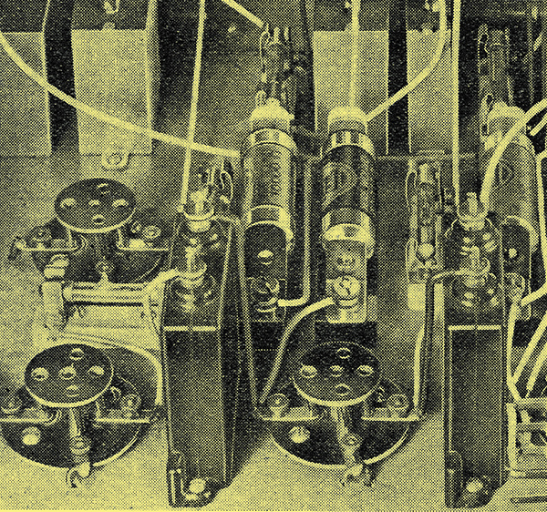
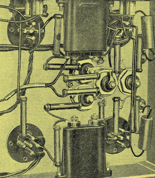
A typical high-quality amplifier of a few years ago - the coupling capacitors can be seen between the valve-holders.
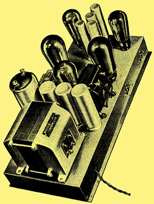
A modern high grade resistance-coupled amplifier.
Actually the wiring above is The Wireless World Push-Pull Quality Amplifier.

A portion of a laboratory amplifier of the battery-operated type.
|